Quantcast
Channel: TI E2E support forums
Viewing all 4543 articles
Browse latest View live

Simplifying radiation-hardened power-supply design with eFuses

$
0
0

Today’s satellites use complex, high-power field-programmable gate arrays (FPGAs) and processors, challenging power-supply design engineers to create robust power supplies. Many designers end up with complicated designs meant to achieve redundancy (the duplication of critical components to increase reliability), involving dozens of discrete components like field-effect transistors (FETs) to continuously monitor and enable specific power rails.

Since not all of these high-power devices will be on all the time, the ability to turn the power to the payload or processor on and off can not only help simplify designs but also lower power consumption. In addition, if a latch-up or a transient occurs in a power device, power-supply designers have to consider how to contain that failure until power can be restored to that rail, or have a redundant power rail take over.

Using an eFuse to simplify your design

Discrete metal-oxide semiconductor FETs (MOSFETs), comparators, amplifiers and references that provide input power to the satellite payload are just some examples of devices that are needed to achieve redundant inputs to the satellite payload, with appropriate monitoring and protection. This type of power-supply design implementation results in larger solutions with many potential radiation and electrical failure points. Figure 1 shows an example of such a complex implementation.

Figure 1: Discrete implementation of a load-switch redundancy application with reverse-current protection, overvoltage protection and overcurrent protection

An eFuse like the TPS7H2201-SP load switch has additional monitoring and protection features like reverse-current protection, over- and undervoltage protection, programmable current limiting, fault timer, and configurable rise time. It can reduce complex designs down to a single monolithic, radiation-hardened device.

Cold sparing

In the event of a complete failure, if there are two fully autonomous power supplies, an eFuse can enable one power supply and turn off the other. This configuration is known as cold sparing, and provides protection for both downstream and upstream components. Figures 2 and 3 show different implementations of cold sparing.

Figure 2: Cold sparing (redundant input voltages) with the TPS7H2201-SP eFuse, including RCP, OVP, OCP, and automatic reset of a tripped power rail

Figure 3: Cold sparing (redundant input and output voltages) with eFuse, including RCP, OVP, OCP, and automatic reset of a tripped power rail

While it is possible to achieve simple on/off functionality with a MOSFET controlled by a processor, a critical component for reliable operation is the reverse-current protection. Reverse current (VOUT> VIN) can occur in cold sparing applications when the secondary switch is off. A design with two FETs back to back can protect against the reverse current propagating to upstream components. TI’s TPS7H2201-SP dual-FET design allows for reverse-current protection when the device is enabled or disabled, a necessary feature for a highly reliable point-of-load power design. Other discrete or integrated load switch solutions available on the market may use a single FET design, and are limited in reverse-current protection capability.

Failure containment

To ensure a power-supply design with dependable performance, another key design consideration is failure containment. The goal of failure containment is to prevent a random failure (like a short circuit or radiation-caused transient) from propagating to downstream components (like an FPGA, data converter or interface device). Placing an integrated eFuse downstream from a critical power component (Figure 4) can help contain failures. An eFuse with programmable current and voltage limits will help enable the detection of overvoltage or overcurrent events so that they do not propagate to downstream components.

Figure 4: Downstream eFuse with overvoltage protection

Conclusion

Adding functionality to monitor critical payload power components (like a DC/DC converter) and planning for failure with redundancy for input components can help ensure a power supply that can withstand harsh environments. Instead of complex circuitry with several active components and increased processor involvement, devices such as the TPS7H2201-SP integrate the functionality of the switch FETs, overvoltage protection circuitry, overcurrent protection circuitry, reverse-current production circuitry, and programmable voltage and current limits in a single device. Additionally, the Qualified Manufacturers List Class V-radiation-hardness-assured eFuse is fully characterized for low-earth-, medium-earth- and geosynchronous-orbit missions.

Additional resources:


A history of industrial Ethernet protocols and their benefits

$
0
0
Every industrial Ethernet protocol has a unique history and differing benefits for industrial applications. In this article, I’ll provide a brief overview and key benefits for three key protocols: EtherCAT, Profinet and multiprotocols. Industrial...(read more)

Overcoming challenges for backlight LED drivers in automotive display solutions

$
0
0

High resolution and seamless operation are important for larger automotive display screens, shown in Figure 1, as consumers want a clear picture with smooth functionality. Given the harsh environments in vehicles, system reliability and safety are also concerns. As a result, it’s a challenge for designers to find a backlight LED solution that’s designed for larger screens while also providing a high dimming ratio and ensuring system safety.

Figure 1: Automotive display with an LCD screen

To drive larger display screens, backlight LED drivers must have a high boost voltage and high current sink. Typically, automotive displays need to be greater than 1000 nits, which requires more LEDs or brighter, higher-current LEDs to achieve this level of brightness. Using more LEDs leads to higher boost voltage, while using stronger LEDs leads to more current. Using an external switching field effect transistor (FET), shown in Figure 2, will provide higher power density to manage a larger-sized panel. Additionally, with an external FET, the power dissipation is spread further from the IC, enabling the thermal rise to be lower. A multichannel driver with a high current low-side current sink is also necessary to drive uniformity of display across the different channels.

TI’s six-channel LP8866-Q1 automotive backlight driver maximizes power density and features an external switching FET. The device, designed for applications such as infotainment systems and head-up displays, offers a current sink as high as 200 mA. A high current sink is beneficial to ensure you will always have sufficient levels of brightness in your display – making it easy to read even on the sunniest days.

Figure 2: Automotive backlight LED driver topology

To achieve a smooth transition of brightness over a wide range, pulse width modulation (PWM) dimming is necessary and should have high resolution – especially in low-light situations. In bright conditions, analog dimming would be a better choice in order to avoid boost output ripple and audible noise issues.

TI uses an adaptive dimming control solution, known as hybrid dimming, illustrated in Figure 3. The LP8866-Q1 can begin dimming with 12-bit current digital-to-analog converter steps from 100% (0xFFFF) to 12.5% (0x2000) input brightness. Below 12.5% brightness, up to 16-bit PWM resolution can be achieved with the device (PWM duty control plus dither control). The benefits of hybrid dimming include reduced electromagnetic interference, lower boost output ripple and audible noise, improved LED optical efficiency, and an increased dimming resolution ratio for a given LED PWM frequency.

Figure 3: Hybrid dimming mode

Additional resources


Automotive exterior lighting gets a major upgrade

$
0
0

Exterior lighting, primarily used to illuminate ground areas near the door, can now be transformed into a projection system used for both vehicle communication and unique styling features.

A small lighting module utilizing the automotive grade DLP3021-Q1 digital micromirror device (DMD) can display an endless number of patterns in any color imaginable. OEMs are not only excited about the styling and customization possibilities features enabled by this product, but also by the possibility of the module to display warnings and alerts to the driver, pedestrians or nearby vehicles.

Download our whitepaper, available here, to learn more about the endless possibilities for exterior small lights designed with the DLP3021-Q1 DMD. Happy designing!

3 common questions when designing with high-speed amplifiers

$
0
0

Not all amplifier designs are created equal, and it’s important to be familiar with common specifications and understand certain concepts when designing with high-speed amplifiers. In the context of this article, high-speed amplifiers refer to operational amplifiers (op amps) with a gain bandwidth product (GBW) greater than or equal to 50 MHz, but these concepts can apply to lower-speed devices as well. Here are some common questions designers have when using high-speed amplifiers.

Q: Why do some high-speed op amps have a minimum gain specification?

A: Decompensated op amps have a closed-loop minimum gain stable specification, but offer a wider GBW and lower noise – for the same current consumption – as their unity-gain-stable counterparts.

“Decompensated” simply means that there is a second pole above 0 dB placed in the Aol (open-loop gain) response curve. This second pole also dictates the minimum gain required to ensure the amplifier’s stability. Think of the Aol curve being “shifted up,” as shown in Figure 1. The increased Aol results in a wider bandwidth.

Figure 1: Open-loop gain response curve for decompensated amplifiers

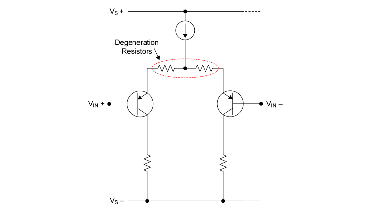
Reducing the size of the degeneration resistors in the input pair of the amplifier increases Aol, as illustrated in Figure 2. Smaller degeneration resistors also help reduce amplifier noise.

Figure 2: Degeneration resistors in an op amp

The OPA858 and OPA859 are two examples of a decompensated and unity-gain-stable amplifier, respectively. For the same current consumption, the OPA858 has wider bandwidth and lower noise, as shown in Table 1.


OPA858

(Decompensated)

OPA859

(Unity gain stable)

Quiescent current (IQ)

20.5 mA

20.5 mA

Gain Bandwidth (GBW)

5,500 MHz

900 MHz

Voltage noise (Vn)

2.5 nV/√Hz

3.3 nV/√Hz

Slew rate

2,000 V/μs

1,150 V/μs

Minimum gain (Acl)

7 V/V

1 V/V

Table 1: Comparing decompensated and unity-gain-stable amplifiers

In addition to increased bandwidth and lower noise, the decompensated architecture also enables a higher slew rate. Overall, the minimum gain specification offers a trade-off in performance that you can take advantage of if you can forego unity gain and meet the minimum gain requirement. Examples of applications where it’s possible to easily meet the minimum gain specification include current-sensing circuits that measure a voltage across a shunt resistor, gain stages in a signal chain and transimpedance circuits.

Q: What are current feedback amplifiers?

A: Current feedback amplifiers are op amps that feed back a portion of the output signal as current in order to control the amplifier. Current feedback amplifiers differ from voltage feedback amplifiers that rely on feedback in the form of a voltage. Most designers are familiar with voltage feedback architectures because they are more common and emphasized in most electronics curriculums.

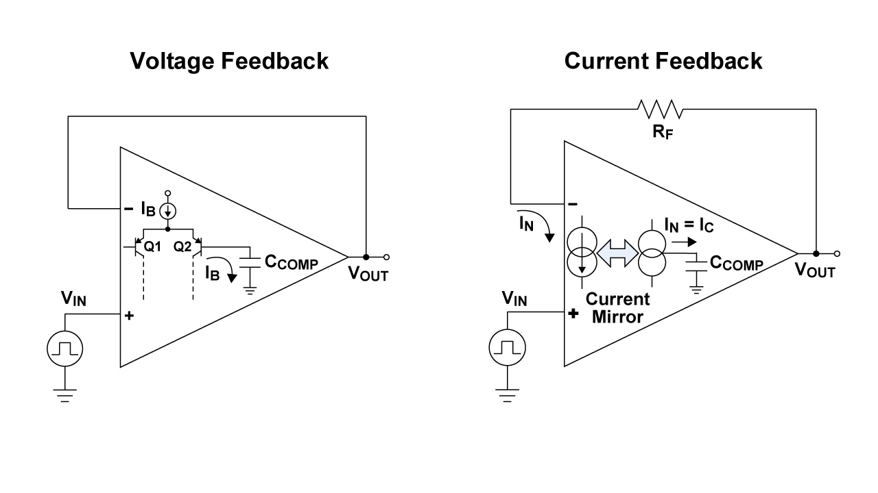
Figure 3 offers a basic input-stage comparison of voltage and current feedback amplifier architectures, where the voltage feedback amplifier is modeled as a voltage-controlled voltage source and the current feedback amplifier is modeled as a current-controlled voltage source.

Figure 3: Comparing voltage and current feedback op amp architectures

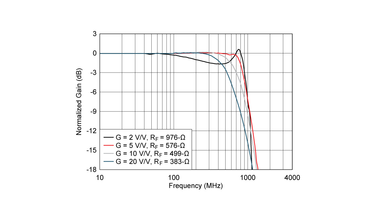
Both architectures are still used as error amplifiers in a negative feedback circuit, but the type of feedback they require is what differs. You can use either amplifier type in inverting and noninverting gain configurations, for instance. One distinct advantage of the current feedback architecture is that the bandwidth is not dependent on the gain. In the voltage feedback architecture, however, as the gain increases, the bandwidth decreases, as shown in Equation 1:


In the current feedback architecture the bandwidth remains nearly constant regardless of the gain, as shown in Figure 4. This graph appears in the THS3491 data sheet.

Figure 4: Gain and bandwidth relationship of a current feedback op amp

Table 2 compares some of the main differences between voltage and current feedback amplifiers.


Voltage feedback amplifier

Current feedback amplifier

Bandwidth

Bandwidth varies with gain

Almost constant bandwidth over gain

DC accuracy

Good

Poor

Output swing

Many rail-to-rail output options

Larger headroom needed for output

Distortion

Better low-frequency distortion

Better high-frequency distortion

Slew rate

Limited slew rate

Very high slew rate facilitating high full-power bandwidth

Gain stability

Restriction on the minimum stable gain for decompensated amplifiers

Stable across gains if feedback transimpedance remains constant

Noise

Low input-referred voltage and current noise

Higher input-referred current noise (unequal for inverting and noninverting inputs)

Typical applications

Applications requiring DC precision

Pulse-oriented applications

High-speed and precise analog-to-digital converter (ADC) interfaces

Transimpedance applications

Digital-to-analog converter interfaces

Output drivers

High-speed ADC interfaces

Sallen-Key filters

Table 2: Comparing voltage feedback and current feedback amplifier applications

Note that current feedback amplifiers are not meant to operate without a resistor in the feedback path. A current feedback amplifier data sheet will suggest specified values for RF; these values are important because the value of RF dictates the compensation of the amplifier, even in unity gain. Like Figure 4, Table 3 is from the THS3491 data sheet. 

Table 3: Example of recommended values for RF from the THS3491 data sheet

For more details about the differences between these two architectures, check out Understanding Voltage Feedback and Current Feedback Amplifiers. You can also learn more about current feedback architectures by watching the TI Precision Labs online training videos.

Q: Why does my high-speed amplifier oscillate when I put it on a breadboard?

A: Generally speaking, it’s likely that the inductance of the package leads as well as the breadboard’s capacitance and inductance are causing your high-speed amplifier to oscillate. Similarly, when designing with high-speed op amps, it’s important to minimize capacitance and inductance on printed circuit boards (PCBs). Even devices on the lower end of the high-speed amplifier GBW spectrum, like the 50-MHz OPA607, require these types of board-level design considerations.

Here are some ways you can optimize your high-speed layout design:

  • Minimize trace length. Minimizing the trace length reduces additional capacitance and inductance.
  • Use solid ground planes. Solid ground planes are generally a better choice than a hashed plane for high-speed designs.
  • Cut out ground planes under signal traces. Removing the ground plane metal underneath the input and outputs of the device helps reduce parasitic capacitance on sensitive nodes.
  • Minimize vias on signal paths. Vias increase inductance and can cause signal fidelity issues at frequencies greater than 100 MHz. To mitigate signal fidelity, route critical signals on the same layer as the amplifier in order to eliminate any vias.
  • Optimize return current paths. Signal trace layout design should minimize the overall signal-loop area and thus minimize the inductance.
  • Properly place and route bypass capacitors. Place bypass capacitors as close as possible to the amplifier on the same layer of the board. Use wider traces and route vias into the bypass capacitors and then to the amplifier – not between the capacitors and the amplifier.
  • Properly place resistors. Place gain-setting, feedback and series-output resistors close to the device pins to minimize board parasitics.

When evaluating the performance of high-speed op amps, it’s best to use the designated evaluation module for a particular device. These boards demonstrate good high-speed board layout design and use SMA connectors to maintain a high-fidelity and impedance-controlled signal path. For more details on high-speed board layout practices, you can read High Speed PCB Layout Techniques.

Overall, high-speed op amps operate much like their lower-speed counterparts. By considering just a few design nuances, you can take advantage of all of the speed and performance benefits that they offer for your system. Which of these questions were most relevant to you? Leave a comment below.

Meet airline restrictions with power-path control for dual batteries

$
0
0

With the Federal Aviation Administration restricting the size of batteries allowed on airplanes, it can be challenging to design applications with batteries down to 100 Wh. Some companies design applications using two small batteries instead of one to meet the regulations, but having two batteries often requires the implementation of redundant or duplicate power supplies, which increases power-path design complexity.

In this article, I will present a simple yet effective configuration to share the load current between multiple power supplies or batteries using two TI LM74700-Q1 ideal diode controllers. This configuration enables you to use multiple batteries or power supplies in your systems and is appropriate for applications such as oxygen concentrators, laptops and portable oscilloscopes.

For systems that include multiple batteries, the load-sharing configuration shown in Figure 1 can dramatically increase battery life because each battery supplies only half of the total load current at a time.

Figure 1: A system block diagram with multiple batteries

Figure 1: A system block diagram with multiple batteries

Supplying only half of the total load current reduces the I2R across the batteries’ internal impedance by a factor of 2, as shown in Equations 1 and 2:

Equations 1 and 2Design verification

When implementing multiple batteries in a system, you cannot assume that two batteries that seem the same are exact copies of each other. They may have different internal impedances or discharge at different rates, which may cause backfeeding or a battery that sources no current. Using the LM74700-Q1 enables each battery to source current proportional to its voltage.

To illustrate this capability, Figure 2 shows the current draw from two 9-V batteries sourcing a constant current load. One battery was new and the other had been partially drained.

Figure 2: Current draw from two 9-V batteries

Figure 2: Current draw from two 9-V batteries

As you can see in Figure 2, the higher-voltage battery sources slightly more current than the lower charged battery. Then, as the higher-voltage battery discharges, its voltage lowers such that it converges with the second battery. Both batteries then begin to supply approximately the same amount of current to the load.

Design considerations

The LM74700-Q1 has an integrated charge pump, which enables the LM74700-Q1 to control N-channel field-effect transistors (FETs) that see as much as 65 VDC across them. The charge pump is able to fully saturate the FETs with a gate voltage up to 15 V above the source.

Implementing an ideal diode controller that uses N-channel FETs as opposed to P-channel FETs is a good fit for battery-powered systems (or any efficiency-driven system). An N-channel FET will typically have a lower RDS(on), a smaller package and a lower gate-charge threshold than a typical P-channel FET with similar voltage ratings. Having a lower RDS(on) FET will further reduce I2R losses in a system’s power path, and a lower gate-charge threshold will enable the FETs to turn on and off more quickly.

To minimize losses and optimize the transient response, proper FET selection is important. Using a LM74700-Q1 ideal diode controller greatly reduces DC conduction losses compared to losses when using a Schottky diode or even P-channel FET implementations. There are a few key parameters to consider when selecting the right N-channel FET for your design, however. If you need the FETs to toggle on and off quickly, then inspect the gate charge (Qg) parameter specified on most TI N-channel FET data sheets. The relationship between the Qg and gate-drive current (Ig) to the time it takes to toggle a FET on and off can be seen in Equations 3 and 4:

Equation 3

Equation 4The gate-drive current for the LM74700 is 11 mA and the gate-sink current is 2,370 mA. Having such a high lg can lead to a faster response time for a system, whether it is a turnon and turnoff command or a reaction to a higher voltage detected on the output. A fast transition ensures that your batteries are protected from any overvoltage events on the output and minimal holdup capacitance is required when transitioning between battery power and a DC power source.

In order to have a balanced current draw on multiple power supplies used in a system, an equivalent resistance in the discharge path is important, as shown in Figure 3. Having a difference in voltage or resistance between batteries will affect the ability to equally source current.

Figure 3: Schematic of an equivalent resistance in the discharge path

Figure 3: Schematic of an equivalent resistance in the discharge path

As you can see in Equations 5 and 6, even if the same source voltages exist in a system, a difference in series resistance can vary the amount of current they will provide. Consider this possibility when implementing systems with multiple chemistries or ages, as they may have different internal impedances.

Equations 5 and 6

Conclusion

Using LM74700-Q1 ideal diode controllers to manage the discharge path for systems with multiple batteries or power supplies can provide a simple and effective methodology. An ideal diode controller helps create an efficient and quick reaction path, especially compared to systems using diodes or P-channel FETs in a similar control scheme.

Building high-performance flow transmitters using the PWM technique

$
0
0
Sensors measure the processes in factory environments to control the conditions in the overall system through the programmable logic controller (PLC). Typical measurements are temperature, pressure, flow and level. There are different techniques that...(read more)

Using DC/DCs buck converters to power modern safety features in commercial vehicles

$
0
0

This article was co-authored by Zach Imm.

Driver and pedestrian safety is a top priority for engineers working on vehicles today and in the future, both partially and fully autonomous. According to recent statistics, more than 73% of traffic accidents, especially for commercial vehicles, are caused by visual blind spots, cellphone use, driver fatigue and driver negligence. Studies show that equipping vehicles with advanced driver assistance systems (ADAS) such as lane departure warning and automatic emergency braking can reduce accident rates by more than 80%, because these systems are an effective way to help drivers eliminate common driving mistakes.

Governments in many countries have issued regulations mandating the installation of ADAS and other advanced security features in commercial vehicles (Figure 1). These features include blind-spot detection, adaptive cruise control and lane departure warning. For those of you designing automotive systems, this means adding more sensors (radars and cameras) and high-performance processors, which in turn means that you need to find a way to supply more power (more than 15 W) in the same printed circuit board area.

Figure 1: Commercial vehicle on the road

2-A to 3-A current rating was enough for a first-stage DC/DC buck converter in ADAS until now. With the increased number of sensors and radars, 4 A, 5 A or even higher current ratings are becoming a real need. Such high ratings pose a big challenge for the power density and thermal performance of the first-stage DC/DC buck converter, especially in a commercial vehicle’s internal battery, which typically needs a 24-V input voltage. As such, you might consider using buck controllers for this type of application given their excessive current capability (more than 10 A). Yet, their larger solution size (plus the need for two external metal-oxide semiconductor field-effect transistors) presents some design limitations. You might also consider nonsynchronous buck converters with an external diode. Remember, however, that a diode increases solution size and design cost, and increases electromagnetic interference (EMI).

In addition, every automotive electronic system is subjected to wide-input-voltage variations during cold-cranking and load-dump conditions. When starting (“cranking”) a cold engine, the 24-V battery voltage will drop to as low as 6 V. A load dump occurs when the vehicle battery is disconnected from the alternator while the battery is charging, which causes a surge in the power line. After shunting the surge with a semiconductor transient suppressor, in many cases your regular first-stage buck converter has to absorb more energy than what the nominal battery voltage provides. This means the wide input range of first-stage buck converter is needed to avoid damaging the whole system by the lower surge from battery after shunting. Normally, the battery voltage will be clamped to 55 V in a 24-V battery system, even with a semiconductor transient suppressor.

To address some of the issues resulting from dealing with high currents, the 3.5-VIN to 60-VIN 5-A LM76005-Q1 synchronous DC/DC buck converter could be a better option. Normally, in 24-V battery ADAS, the large dropout voltage (24 VIN and 5 VOUT) in full load conditions will cause challenges in thermal management for a synchronous DC/DC buck converter solution (such as higher temperature in a larger dropout voltage), which will limit the actual loading capacity of the DC/DC buck converter. To address this thermal issue, the LM76005-Q1 is packaged in a 4-mm-by-6-mm 30-pins very thin quad flat no-lead (WQFN) package with a thermal pad (1.8 mm by 4.5 mm) and wettable flanks (Figure 2). The large thermal pad and high efficiency help optimize thermal performance (Figure 3).

Figure 2: LM76005-Q1 schematic

Figure 3: LM76005-Q1 efficiency (VIN = 24 V, VOUT = 5 V, IOUT = 5 A, FSW = 400 kHz)

With the higher current requirements of new ADAS, you may worry about increasing EMI of the entire system. Therefore, it’s important for your chosen DC/DC buck converter to meet EMI Comité International Spécial des Perturbations Radioélectriques (CISPR) 25 standards for both peak and average EMI limits. The LM76005-Q1 features optimized switching edges that enable faster switching with no ringing and an internal ground plane, which combined with the flip-chip on-lead frame QFN package minimizes EMI and electromagnetic compatibility (EMC) emissions (Figure 4) and easily passes the CISPR25 Class 5 automotive standard.

Figure 4: LM76005-Q1 radiated EMI (VIN = 13.5 V, VOUT = 5 V, IOUT = 3 A, FSW = 400 kHz)

Conclusion

There is no doubt that ADAS improves driver safety. With the success of these systems, you can expect an increase in the integration of even more sensors into automotive designs. Amid a continual focus on high reliability, higher current capability, better thermal performance and lower EMI/EMC emissions, knowing the key considerations for choosing wide-input-voltagebuck converters and how to integrate them seamlessly into the power-management circuit can help give your ADAS designs an edge.

Additional resources

Read these technical articles:


Overcoming common design challenges in an UV sterilization box system

$
0
0
An ultraviolet (UV) sterilization box is designed to use UV rays to kill bacteria. UV LEDs can produce UV rays of 260 nm to 280 nm, which can break the bacteria DNA/RNA strand and kill bacteria completely, with a sterilization rate as high as 99%. LED...(read more)

Enabling IIoT to reach beyond the factory floor

$
0
0
Internet of Things (IoT) and industrial Internet of Things (IIoT) have become synonymous with connected factories and making traditional factories smarter in order to reap the benefits of greater efficiency. Today, it’s becoming more common for...(read more)

Six key questions when designing for USB protocol interfaces

$
0
0

Designing a system that uses high-speed signals for data transmission can be difficult, especially when there are so many available communication protocols. While many are ideal for high-speed signals, one in particular continues to grow in popularity – the USB. Often been associated with gaming, automotive head unit, and PC and notebook applications, the USB protocol has become a more general-purpose high-speed data protocol, connector and cable specification due to its support for multiple types of data transfers and high-power charging. Figure 1 shows the evolution of USB since it's release in 1998.

Figure 1: The history of the USB protocol through release of USB 4.0 in 2019

To help you understand whether the USB protocol is a good fit for your system and meets your high-speed interface needs, here are six key questions designers should consider.

1: What are the interface capabilities of your CPU or MCU?

When working with USB, it’s important to first consider the interface capabilities of your central processing unit (CPU) or microcontroller (MCU), as this device is fundamental for high-speed data transfer in your design. If you find that you need to transmit data from a CPU or MCU to a connected peripheral with a data rate greater than 10 Mbps, USB can be a great fit.

2: How do you transmit data over a long distance when your interface’s data link reliability is lacking?

USB could replace this connection with an existing integrated circuit solution for extending your interface’s communication abilities. USB redrivers help maintain signal integrity while transmitting over long distances. Devices like the TUSB216 (USB 2.0) and TUSB1002A (USB 3.0) include features specific to the USB protocol that ease the implementation of redrivers in USB.

3: What if your MCU or CPU has only one instance of the USB interface?

The USB includes devices called USB hubs that can turn one port into multiple ports with minimal effort. Four-port high-speed USB hubs such as the TUSB4041I, TUSB8041A and TUSB8042A can help increase the number of devices that can be used at once.

4: What if your CPU or MCU interface has limited interface options?

USB solutions have progressed, enabling conversion to other interfaces like universal asynchronous receiver-transmitter (UART) or Serial Advanced Technology Attachment (SATA). USB bridges enable the conversion of USB to UART and SATA. If your MCU or CPU does not have an interface to UART or SATA, or if the transmission distance is too great for plain UART or SATA interfaces, consider USB bridges like the TUSB3410 and TUSB9261.

5: Do all USB connections require external connections?

While you may see external USB ports everywhere in consumer products, USB connections do not have to be external. If your chosen MCU or CPU has USB capability, you can also consider USB for embedded connections to other MCUs or CPUs in your system. USB has built-in data encoding to help reduce electromagnetic interference and link power management for power efficiency. USB also adds flexibility for customer software where many low-level drivers already exist today.

6: What if you need more flexibility than what standard USB connections provide?

The introduction of the USB Type-C® protocol has greatly increased USB’s flexibility. USB Type-C enables the creation of peripherals that act as a USB host or USB device, enabling systems to react to different kinds of connections in multiple ways. USB Type-C active multiplexers can also help ensure the correct configuration of the interface while providing signal integrity compliance to the USB specification.

Active multiplexers such as the TUSB542 and TUSB1042I should be used in your standard Type-C designs. USB Type-C also facilitates the transmission of additional types of high-speed data such as DisplayPort, High-Definition Multimedia Interface, UART, and other video or custom interfaces over the same connector. The TUSB1146 and TUSB1064 are essential for systems to enable their Alternate Mode capabilities.

For technical details on the USB protocol and USB implementations, check out the resources below, or post on the TI E2E Interface forum if you have a technical question about USB and need help picking the correct product for your system.

Additional resources

Exploring advancements in industrial and automotive markets with 60-GHz radar

$
0
0
In just a few decades, the world has seen the replacement of human-operated machinery and vehicles with intelligent versions now operated autonomously or with less human intervention. With such rapid growth, the industrial and automotive markets have...(read more)

Selecting the right processor for your data concentrator design

$
0
0
A trend in the rapid growth of smart grids is enabling more intelligent functions in residential equipment, such as smart electricity meters and data concentrators. A smart grid requires a multi - communication approach to analyze grid status, detect...(read more)

Benefits of rechargeable batteries in real-time location system trackers

$
0
0

Real-time location systems (RTLS) enhance the lives of consumers and businesses by making everyday routines smarter through accurate, location tracking technology such as GPS and Bluetooth® Low Energy. RTLS trackers eliminate the stress of losing belongings such as luggage or pets using long-distance GPS tracking. RTLS trackers also enhance businesses with Bluetooth® Low Energy beacons to monitor customer traffic, employee patterns and the location of equipment, which can help identify process bottlenecks and improve customer experience. These applications are just the beginning for RTLS trackers, and designing RTLS with rechargeable batteries can help you get the most out of the systems.

In this article, I will highlight the benefits of rechargeable batteries in RTLSs and explain how TI chargers solve design challenges associated with implementing rechargeable batteries in RTLSs.

The benefits of rechargeable RTLS

Rechargeable RTLS designs are useful in large-scale applications with devices that do not have access to a direct power supply. The area design advantages of RTLSs such as:

  • Eliminating the need to buy and replace hundreds of primary cell batteries.
  • The freedom to place devices anywhere with no need for a direct power source.
  • The ability to maximize possible device locations by creating smaller designs through the implementation of compact charger integrated circuits (ICs).

In addition to large-scale applications, rechargeable RTLS is advantageous in consumer electronics, such as personal item tracking devices and smart dog collars. With rechargeable RTLS, customers can:

  • Fully charge a battery in five hours.
  • Never worry about losing their keys, wallets or pets because the batteries in the RTLS are dead.

Figure 1 highlights different applications of rechargeable RTLSs.


Figure 1: Rechargeable RTLS applications

Rechargeable RTLS design challenges

Indoor and outdoor RTLS devices are usually designed to be aesthetic and small for portability, and designing your system with power integrated battery chargers helps achieves those two design requirements. Chargers with power integration include power rails on the device, such as an LDO, load switch and low power buck convertors, which provide the correct voltages for other components in the circuit. Incorporating power rails into the charger reduces the overall number of components and helps you achieve small, aesthetic designs.

Due to the need for small, portable devices, the batteries in RTLS devices are on the smaller side because of the size constraints, and the devices also need to be designed to maximize the capacity of the battery. Chargers with easily customizable charge currents and accurate termination currents help maximize the lifetime of the battery. The I2C interface allows you to easily set the charge current to a small value that will charge the battery quickly without damaging it which increases the number of times the battery can be recharged. Accurate termination currents help prevent higher termination currents that cause a reduction in the length of each charge and unused battery capacity.

Finally, it requires effort and labor costs to collect and recharge RTLS devices, especially for large-scale applications, so designing your device with efficient power consumption is critical. Choosing a charger with very low quiescent current minimizes power consumption and increases battery time. In addition, chargers with load switches can cut off power to blocks that are not being used which also reduces power consumption.


Figure 2: Rechargeable RTLS block diagram for pet trackers

TI chargers for rechargeable RTLS devices

TI’s BQ24040 and BQ21061 are two linear chargers that can help address common design challenges. The BQ24040 satisfies charging requirements for simpler RTLS devices. It is 4mm2 and its 1µA standby current helps extend battery life leading to more uptime. This device is useful for RTLS applications in which people rarely interact with the device, such as Bluetooth® Low Energy beacons. The BQ21061 is useful in RTLS devices such as smart dog collars. The I2C interface enables easy configuration of charging properties, while the LDO adds an extra power rail to minimize space. The power path feature provides a ship-mode option.

The BQ25619 is a switching charger that would also be useful in rechargeable RTLS applications. In general, switching chargers are more efficient than linear chargers in terms of power loss; they also have higher charging currents and wider input voltage and current ranges. A switching charger, like the BQ25619, is a good fit for rechargeable RTLS applications that need bigger rechargeable batteries and fast power consumption. The BQ25619 has a flexible 20-mA to 1.5-A charging current range and quick charge capabilities, along with I2C for charging customization and a standby current of 10 µA to preserve battery life. Table 1 compares all three chargers.

FeatureBQ24040BQ21061BQ25619
Standby current1 µA470 nA10 µA
Ship modeNoYesYes
Charge current range100 mA - 1 A1.25  mA - 500 mA20 mA - 1.5 A
Standalone or I2CStandaloneI2CI2C
Size2.00 mm x 2.00 mm2.00 mm x 1.60 mm4.0 mm x 4.0 mm
Power pathNoYesYes
LDONoYesNo

Table 1: Comparing the BQ24040, BQ21061 and BQ25619 battery chargers

In addition to the previously mentioned applications, herd tracking is a growing opportunity for RTLSs that requires a large-scale solution for animal tracking. By placing RTLS devices similar to the dog collars on farm animals such as cows, farmers are able to monitor the health and location of every animal in a herd to make smarter, more informed decisions. Designers for this application are implementing highly integrated chargers with long battery life, such as the BQ25155, in order to efficiently collect biometric data. As the need for RTLS continues to grow, design engineers are turning to highly integrated battery chargers to keep up with more demanding device requirements.

Additional resources

Introduction to the fundamental technologies of power density

$
0
0

The importance and value of power density in modern power-delivery solutions cannot be overstated.

To better understand the fundamental technologies of high-power-density designs, in this article I’ll examine the four most important aspects of high-power-density solutions:

  • Reduced loss generation.
  • Optimal topology and control selection.
  • Effective heat removal.
  • Reducing system volume through mechanical and electrical component integration.

I’ll also demonstrate how partnering with TI, and using advanced technological capabilities and products that support these four aspects, can help improve your efforts to achieve high-power-density figures.

But first, let’s define power density and highlight some important details when comparing solutions based on their power-density figures.

What is power density?

For power-management applications, the definition of power density seems straightforward: it is the rated (or nominal) output power of the converter divided by the volume that the converter occupies as shown in Figure 1.

Defining nominal power and volume in power density

Figure 1: Calculating power density is easy, but how nominal power and volume are defined can often lead to ambiguity.

But even this simple definition demands a lot of clarification if you want to compare power supplies, based on their power-densities.

The output power corresponds to the continuous output power that the converter can deliver under worst-case environmental conditions. The relevant power capability may be affected by a combination of ambient temperature, maximum acceptable case temperature, orientation, altitude and expected lifetime.

Similarly, you can define the volume of the power supply in many different ways, depending on the converter’s application and construction. Some of the variables that can significantly impact the volume – and, consequently, the reported power density of the power supplies – are the inclusion or exclusion of electromagnetic interference filters, fans, housing requirements, and input and output energy-storage capacitors, which are often required but not part of many modularized power supplies. Therefore, it is imperative to know and consider these variables when comparing reported power-density data from the literature.


Learn more about the limitations to increasing power density and how to overcome them.


Read the white paper now

History of power density

Let’s have a short historical overview, looking at where the fascination with power density comes from and how this trend began.

Efficiency was a driving force of innovation in power technology since the early days of switched-mode power conversion. Switched-mode power converters made it possible to break the deterministic efficiencies of linear power supplies, which were primarily dependent on input and output voltage ratios and few available topologies.

The need to improve efficiency has accelerated significantly since the early 1990s, fueled by personal computing and electronics, telecommunications, and advancements in semiconductor technology. The increased efficiency of the power solutions has been facilitating a continuous progress in power density as well, as depicted in Figure 2.

Figure 2: Efficiency and power density are closely coupled in power-delivery applications.

Many waves of energy crises and the consequent emergence of regulatory requirements made efficiency an even more important attribute for power systems, specifically energy conservation and total cost of ownership.

During the last decade, high power density has become recognized as the ultimate pinnacle of power-system engineering.

How to achieve high power density

To better understand the focus on power density, let’s look at what it takes to achieve high power density. The special relationship between efficiency, size and power density is immediately apparent – even for casual observers.

Efficiency is considered the gatekeeper of achieving high power density because it’s imperative to reducing the amount of heat from a device. To take advantage of higher efficiency, a solution’s volume – its size, in other words – must shrink. Achieving both high efficiency and small size at the same time requires a solution that can work efficiently at high operating frequencies. In particular, such a solution should include:

  • Reduced switching losses. A switching element that can provide low conduction andlow switching losses.
  • Topology, control and circuit design. You need the right topology to operate at high switching frequencies. Control methods and innovative circuit implementations are also important, considering that most converter topologies can operate in different modes – such as traditional square-wave pulse-width modulation, zero-voltage or zero-current transition, or full-resonant mode – based on the applied control technique.
  • Integration. The scaling effect of the higher operating frequency on passive components can shrink the size of a power converter. But there’s another very important piece of the power-density puzzle – integration – happening in the silicon technology itself through the monolithic incorporation of power and control elements. On the semiconductor device side, designers are using multichip module technology integrating multiple semiconductor dies – and in many cases even passive devices, capacitors and magnetic components. The mechanical and printed circuit board designs of the converters and their enclosures are undoubtedly a crucial factor in achieving high power density.
  • Improved thermal performance. TI’s enhanced packaging and advanced leadframe technologies play an important role in minimizing the temperature gradient between the outside cooling surfaces and the actual silicon temperature. These technologies, together with accompanying modeling and optimization capabilities, offer improved thermal performance that can not only enable high-power-density designs but also long-term, reliable operation of TI’s semiconductor devices.

Applying these four fundamental technologies together is the cornerstone of many successfully executed high-power-density designs. Thus, you can view the power density achieved like a report card that grades how well the designer applied the most appropriate semiconductor technology, and whether they selected the right topology, control method, mechanical design, thermal management and integration strategy.

Conclusion

If you truly want to understand why power density is important — beyond viewing it as a universal score to rank technical merit in power engineering — you have to step back and look at how the industry and society as a whole benefit from higher power density.

For example, smaller physical dimensions usually translate to less raw material usage, which could be indicative of lower material cost. Similarly, a smaller size and fewer materials will possibly result in a lower weight, which is an extremely valuable attribute in power systems in the transportation segment that can lead to fuel savings or longer ranges. And finally, with higher power density comes the possibility of miniaturization. Pushing this aspect to its limits has allowed the power-conversion industry to create previously unimaginable new markets.

As these examples show, power density is important given the well-defined economic advantages for the manufacturer, user or operator at the system level that can result in a lower total cost of ownership.

I hope this information, and our related five-part training video series, will inspire you to learn more about our company and technologies, which can enable industry-leading power densities from power-rail voltages below 5 V all the way to 600 V and above, using our advanced silicon technology and high-voltage gallium-nitride power devices.


Three easy steps to connect and start developing with TI’s cloud-based tools

$
0
0

As soon as you receive a new development kit, you want to get started developing as quickly as possible, right? Searching for all of the right tools and resources can be a daunting task that slows you down – unless the tools you are using could determine the resources you need automatically.

Using TI’s cloud-based development tools, it is possible to plug in your LaunchPad™ development kit to run examples and even develop and debug applications. Here’s how:

  1. When your development kit arrives, go to the TI DevTools page(you’ll also find the URL printed on the board).
  2. Plug in your kit; you will be prompted to install a small software agent that enables the cloud tools to communicate with the kit.
  3. After the tools have identified your kit, you will receive step-by-step instructions on how to begin development.

The TI embedded development portal

Using our project wizard, select “Create project online” from the main portal, which allows you to browse through a listing of available examples and import them into Code Composer Studio™ Cloud. Figure 1 shows the TI Embedded development portal that has detected an connected LaunchPad development kit.

 Figure 1: The TI embedded development portal

Code Composer Studio Cloud

Code Composer Studio Cloud is a cloud-based integrated development environment, as shown in Figure 2. Code Composer Studio Cloud supports building, editing and even debugging of applications. Once you have imported an example project, just click Debug and it will build the example, start the debugger and flash it onto your LaunchPad development kit. This is all possible without having to download a software development kit (SDK) or any additional software, other than the small agent that detects and communicates with the board. The agent will even check if the firmware on the debug probe embedded on the LaunchPad development kit needs an update.


Figure 2: Code Composer Studio Cloud

Resource Explorer

Resource Explorer is a tool that enables you to browse through all of the content within the cloud to find examples and code that best match your application. As shown in figure 3 you can even view the readme file for an example that describes the example and includes any additional instructions.

Figure 3: Resource Explorer

Another advantage of working in the cloud is that you don’t have to worry about not having the latest software, as it defaults to the latest version. There is a wealth of training material available in Resource Explorer to help you get familiar with TI’s devices, tools and software. For SimpleLink™ microcontroller users, SimpleLink Academy is a great place to start.

After selecting an example, using Code Composer Studio Cloud, you can run the application, single-step through the code, set breakpoints and watch variables. Because you are working in a cloud-based environment, you can accomplish these tasks in minutes instead of spending hours setting up a desktop environment.

SysConfig

There is also a system configuration tool called SysConfig. If the example project you are using is SysConfig-enabled, you can use this tool to configure elements of the application such as peripherals, drivers, software stacks and pin assignments. Double-click the configuration file in the project to open SysConfig in your browser.

Prefer desktop tools?

For more intensive development, from the same embedded development portal you can access TI’s desktop development tools, including Code Composer Studio software. The desktop version of Code Composer Studio software also includes Resource Explorer and SysConfig, which gives you access to all of the SDKs and software packages you need for development. You can even export your projects from Code Composer Studio Cloud and then import them into the desktop version.

Conclusion

TI’s cloud-based development tools make it easier to evaluate and start development on a microcontroller. What may have taken most of a day to get started in the past now only takes minutes. With the power of the cloud at your fingertips, what will you create? Grab your LaunchPad development kit and go to the TI DevTools page to start developing.

Demystifying medical alarm designs, part 1: IEC60601-1-8 standard requirements

$
0
0
Sanjay Pithadia co-authored this technical article. If you have ever heard the not-so-melodic alarm of a patient monitor in an intensive care unit (ICU) or even on a TV show or movie set in a hospital, you might remember that these alarms have particular...(read more)

Back to basics: Exploring the benefits of affordable Bluetooth® Low Energy

$
0
0

Bluetooth® connects us to the world through our smartphone. We can interface with door locks, thermostats or even our cars. But is all Bluetooth the same? Do you unlock your car with the same Bluetooth that you used to stream music from your phone to a smart speaker?

The answer is yes – and no. Bluetooth Low Energy is a standards-based protocol that enables interoperability between different devices and products; however, there are also optional add-on features to expand the functionality of more complex solutions. There are three basic things that you should consider when picking the right Bluetooth solution for your application: software features, hardware and cost.

Software features

On the software side, there are two important technical details to consider:

  • Which core specification can the device certify to?
  • Which feature set does the device support?

The core specification defines the basic features of Bluetooth Low Energy that must run in order to create the interoperability consumers experience when their phone interfaces to products made by hundreds of different companies. These features are mandatory to release a product that is BTX.X certified (for example, BT5.0). Additional features associated with different Bluetooth Low Energy specification releases (outside of the core specification) are optional. For instance, BT5.0 added a high-speed mode, a long-range mode and extended advertising, but your application doesn’t have to support these features to be BT5.0-certified. Along the same lines, BT5.1 added direction finding as a bonus feature.

Hardware

The hardware that runs the Bluetooth stack can also vary widely. There are basic devices that have a single core for both the application and radio-frequency functionality, versus integrated devices that offer both an application core and a microcontroller (MCU) core. There are also one-time programmable devices that are read-only memory-based and cannot be updated after programming, whereas flash-based devices can be upgraded thousands of times and even upgraded in the field over the air.

If your goal is to design a scalable and reliable application, it is important to evaluate affordable, high-quality devices with various hardware options including integrated application MCUs and flash memory architectures. Such evaluations enable you to select the right feature at the right price.

The table below shows some of the key hardware, software, and pricing tradeoffs between BLE devices in the TI portfolio.


CC2640R2L

CC2640R2F (Q1)

CC2642R (Q1)

CC2652RB

CC2652P


Most cost-effective

Smallest size, lowest power automotive option

Full BT5.1 feature set, automotive option

No need for external crystals – smallest system size

Longest range, highest output power, multiprotocol Bluetooth Low Energy

1 Ku price

$0.85

$1.44

$1.86

$3.00

$3.10

Bluetooth core specification | Bluetooth feature set

BT5.1 | BT4.2*

BT5.1 | BT4.2*

BT5.1 | BT5.1

BT5.1 | BT5.1

BT5.1 | BT5.1

Smallest package option

5-mm-x-5-mm quad flat no-lead (QFN)

2.7-mm-x-2.7-mm wafer chip-scale package (WCSP)

7-mm-x-7mm QFN

7-mm-x-7mm QFN

7-mm-x-7mm QFN

Application MCU core

M3

M3

M4F

M4F

M4F

Flash (KB)

128

128

352

352

352

Maximum output power

+5 dBm

+5 dBm

+5 dBm

+5 dBm

+20 dBm

Protocol support

Bluetooth Low Energy, Proprietary 2.4 GHz

Bluetooth Low Energy

Bluetooth Low Energy

Bluetooth Low Energy + 802.15.4 (Zigbee, Thread)

Bluetooth Low Energy + 802.15.4 (Zigbee, Thread)

*Some limited options available for BT5.0

Table 1: SimpleLink™ Bluetooth Low Energy portfolio offering and specifications

Some applications like wearable devices require the smallest size possible so that they aren’t intrusive. Other applications require higher performance, such as longer ranges or multiprotocol operation, and are not size-sensitive. The TI portfolio offers hardware options that scale across memory footprints, performance, Bluetooth features and package. For instance, the smallest-size offering is the CC2640R2F in the 2.7-mm-by-2.7mm WCSP package. The most cost-effective offering is the CC2640R2L in the 5-mm-by-5-mm QFN package. For multiprotocol support and long ranges, the best option is the CC2652P with its integrated power amplifier.

Cost

When designing a Bluetooth Low Energy product, it is not only important to select the correct features, but also to consider the price. The SimpleLink portfolio has devices with various price, feature and performance options. The newest device in the TI Bluetooth platform, the CC2640R2L, is a flash-based, Bluetooth wireless system on chip with a starting price of $0.85. Additionally, the CC2652RB offers a path to system cost savings by removing the need for external crystals. It integrates this crucial system component into the package of the device, saving $0.10 to $0.20 on average for the total system compared to crystal-based solutions.

Remember – all Bluetooth is standard, but it’s not all the same. When designing your application, it’s critical to cover the Bluetooth basics (software features, hardware and cost) so that you can find the right solution whether you’re unlocking a car or setting the temperature in your house. The TI portfolio is built to cover all bases by offering a variety of software options (BT5.0, locationing, co-existence) and hardware options (memory, package, performance).

Get started today: www.ti.com/BluetoothLowEnergy

How device-level features and package options can help minimize EMI in automotive designs

$
0
0

This article was co-authored by Sam Jaffe.

As automotive systems continue to evolve, the number of applications requiring additional power continues to increase. Engineers designing higher-power systems often switch from low-dropout (LDO) regulators to DC/DC buck converters, given the latter’s improved efficiency and thermal performance. Unfortunately, making this switch comes at a cost, since DC/DC buck converters have considerably higher electromagnetic interference (EMI) than the LDO regulators they replace.

Because EMI can affect sensitive components such as the AM/FM radio receiver and driving-assist sensors, and because significant EMI can actually degrade or even prevent proper system operation, official standards like Comité International Spécial des Perturbations Radioélectriques (CISPR) 25 Class 5 set EMI limits for vehicles and boats with internal combustion engines.

Outsmarting board layout limitations

One of the easiest ways to mitigate EMI is with the right printed circuit board (PCB) layout. For a buck converter, your most important considerations are:

  • Reducing the surface area of high transient voltage (dv/dt) nodes.
  • Reducing the loop area of high transient current (di/dt) loops.

These considerations dictate the placement of certain components that, when done properly, can help minimize EMI.

A board’s size or shape can limit certain component placements, however, and the time and cost required to perform board spins may be prohibitive. So what are your options if you have such constraints but need to remain under CISPR 25 Class 5 EMI limits in your application?

If it’s not possible to optimize your layout for EMI, there are DC/DC converters with layout-agnostic package and feature improvements at the device level that can help mitigate EMI when an EMI-optimized layout isn’t an option.

EMI-friendly device-level features

Spread spectrum is a feature that dithers the switching frequency to spread the harmonic peaks of EMI caused by the switch node. Spreading the energy of the higher harmonic peaks turns tall, sharp emissions into low, smooth emissions, which in turn reduces the amount of filtering and optimization needed for a design to fall under emissions limits.

Slew-rate control reduces the turnon time of the high-side field-effect transistor (FET), which reduces energy in the high-frequency harmonics. Simply add a small resistor in series with the boot capacitor, or use a boot resistor on the dedicated RBOOT pin of devices that have this feature built-in. Slowing the slew of the FETs improves EMI but decreases efficiency, however.

EMI-friendly packages

Package-level features that can help suppress EMI include TI’s HotRod™ flip-chip-on-leadframe package, which has no internal bond wires; see Figure 1. Removing inductive bond wires in the path of the high di/dt loop of the input capacitors’ discontinuous current eliminates a significant source of input loop inductance and satisfies one of the primary considerations I mentioned earlier – reducing the area of high di/dt loops.

Figure 1: Cross-section of a standard wire-bond quad flat no-lead package and a HotRod package

Another package-level feature is the use of a symmetrical pinout for critical paths. DC/DC buck converters such as the LMR33630-Q1, LMR36015-Q1, LM61460-Q1 and LMQ61460-Q1 have a switch-node pin in the center with PGND and VIN on either side.. Such symmetry creates magnetic fields that provide better field containment and reduce coupling to nearby circuits.

Integrated input capacitors

To mitigate EMI even further at the device level, products such as the LMQ61460-Q1 now integrate input capacitors inside the package. Figure 2a represents these capacitors as dark rectangles straddling upper- and lower-right pin pairs VIN and PGND. Refer to Figure 2b for the pinout. Including input capacitors inside the package reduces parasitic inductance, ringing and high-frequency EMI (again satisfying the second consideration). High-frequency EMI is particularly important because problems in the high-frequency range can become worse in the presence of higher input voltages and higher output currents – conditions common in automotive applications.

(a)                                                     (b)

Figure 2: X-ray image of the LMQ61460-Q1 with integrated capacitors (a); LMQ61460-Q1 pinout (b)

EMI does present challenges in automotive applications. But board layout constraints don’t automatically mean that you’re out of options. Device-level features and modern package types offer reliable EMI mitigation techniques so that you can improve your designs and confidently remain under EMI emissions limits.

Additional resources

How to affordably add EtherNet/IP, EtherCAT and PROFINET to an autonomous factory

$
0
0
Remember when science fiction movies would have a scene showing a fully automated factory managed by artificial intelligence? Such factories exist now! An autonomous factory relies on real-time communication between individual components such as motion...(read more)
Viewing all 4543 articles
Browse latest View live


<script src="https://jsc.adskeeper.com/r/s/rssing.com.1596347.js" async> </script>