Quantcast
Channel: TI E2E support forums
Viewing all 4543 articles
Browse latest View live

5 best practices to extend battery life in flow meters

$
0
0

Water and gas meters use lithium manganese dioxide (LiMnO2) and lithium thionyl chloride (LiSOCl2) batteries as energy sources. LiSOCl2 batteries are popular in smart meters because they provide better energy density and a more efficient cost-per-wattage ratio than LiMnO2 batteries. However, LiSOCI2 batteries have a poor impulse response, which can lead to a large drop in voltage during transient current loading.

It is possible to combine buffer elements such as hybrid layer capacitors (HLCs) or electric double-layer capacitors with LiSOCl2 batteries to improve their pulse load capability, but a reliable combination of HLCs and LiSOCl2 batteries is costly and can impact the total cost of the meter. Because the battery also has an impact on the maintenance requirements and lifetime of a meter, an alternative method that combines buck-boost converters with LiSOCl2 batteries can help reduce overall solution costs and extend the lifetime of the meters.

In this article, I will review five best practices when working with buck-boost converters and LiSOCI2 batteries to maximize battery life and reduce overall maintenance and cost requirements. But first, let’s examine some common design challenges.

Key design challenges when designing smart meter systems

A typical smart meter system comprises five key components, including a metrology front end, communication front end, microcontroller (MCU), power-management integrated circuit and protection front end.

In addition to these requirements, water meters usually come in small form factors and must operate for more than 15 years in the field with minimal maintenance.

Power consumption profile for typical flow meters

Table 1 lists the power consumption profile of a standard meter divided into three operating modes.

Operating mode                                                  Origin                                                  

Current range (A)                           

Impact on flow meter energy-management system


Standby mode

Metrology, MCU and protection5 µA to 100 µAThis is the main contributor to the lifetime of the meter. Thus, the efficiency of the supply system should be excellent (> 95%).
Middle stage modeCommunication front end in receiving mode2 mA to 10 mASome asynchronous radio-frequency (RF) protocols such as narrowband Internet of Things require the RF front end to stay in receiving mode. In such cases, supply system efficiency should remain excellent. 
Active modeCommunication front end in transmitting mode20 mA and more This is a main contributor to the degradation of a LiSOCI2 battery. Thus, the supply system should allow the limitation of the peak current drawn from the battery while maintaining good efficiency (>80%). In general, the system is in active mode for 2 minutes every 24 hours, depending on the communication system implemented.

Table 1: Power consumption profile of a standard flow meter

Best practices for designing meters with a buck-boost converter

To help extend the battery life and performance of your smart meter design, consider these five best practices.

Best practice No. 1: Limit the peak current drawn from the battery.

As you can see in Figure 1 (from the data sheet of a SAFT LS17330 battery), LiSOCl2 batteries usually do not support the high dynamic range profiles required by radio communication systems used in smart meters. One approach to overcome this issue is to use the TPS63900 buck-boost converter and a buffer element to filter the battery current.


Figure 1: SAFT LS17330 typical discharge profiles at +20°C

Best practice No. 2: Make the output and input voltage levels independent.

Implementing independent voltage levels optimizes the input current profile drawn from the battery and the output current provided to the load. This practice also simplifies the usage of the buffer element between the input and output.

Best practice No. 3: Use converters with a low operating current and a standby current below 500 nA.

In order to optimize the system’s energy use, the average current consumption of the converter must be negligible in comparison to the current consumption of the system. For example, if the average current consumption of a flow meter is around 5 µA, the converter should have a standby current below 500 nA.

Best practice No. 4: Keep the voltage of the supply system as low as possible.

Think of the system as a resistance supplied by the converter. Keeping the supply voltage low enables a reduction in the standby current consumed by the system.

Best practice No. 5: Optimize voltage load per operating mode with dynamic voltage scaling.

As Figure 2 illustrates, the TPS63900’s dynamic voltage scaling feature enables the converter to change its output voltage on the fly and thereby power the load at its best operating point.


Figure 2: TPS63900 typical application

Some measurements

Let’s take a load transient measurement with these conditions:

  • 158 µA.
  • 999 ms to 97.4 mA.
  • 1 ms, Vi = 3.6 V, Vo = 3.0 V and Co = 300 µF.

As shown in Figure 3 and Figure 4, the TPS63900 is capable of filtering the input current drawn from the battery while maintaining excellent regulation on the output voltage.


Figure 3: The pulse response of the TPS63900


Figure 4: TPS63900 efficiency with an input voltage of 3.6 V

By combining ultra-low standby current consumption, excellent transient response, output noise level, and dynamic voltage scaling in a 2.5-mm-by-2.5-mm package or 21-mm2 total solution size, the TPS63900 can help resolve challenges when working with LiSOCl2 batteries and solved for a long time by conventional, more complex and costly approaches.


Figure 5: TPS63900 solution area

For more information about designing with the TPS63900 buck-boost converter, see the additional resources or comment on this article.

Additional resources


How to design a social distancing and contact tracing solution with Bluetooth® Low Energy

$
0
0

With its low-cost and low-power features, Bluetooth® Low Energy technology has become the foundation for a wide range of applications. One example is using Bluetooth beacons to create a real-time location system, which is a positioning system that can monitor the whereabouts of equipment or people.

So what role does Bluetooth play in this type of application? Asset tracking uses Bluetooth tags that communicate with one another autonomously to both transmit and receive data in order to effectively monitor the proximity of things or people. Why would you want to monitor the proximity of one person to another? These days, when it comes to easily transmitted illnesses, it’s important to take action to safely interact with one another. Whether it’s a personal situation such as going to the gym or grocery store or a business operating with many workers, the practice of proper social distancing applies to everyone.

Using Bluetooth technology for contact tracing and social distancing is a way to effectively monitor and slow the spread of easily transmitted illnesses to encourage safe practices. But how does it work? Let’s take an example scenario of a workplace. Each employee receives a wearable bracelet or tag. The tags can communicate with one another autonomously and alert employees when they are within a given proximity to another tag, thus ensuring proper social distancing. The tag can also collect data when interactions occur such that if an employee tests positive for a given illness, the data can help determine who else may have been exposed. Using proximity detection rather than location detection protects the wearer’s privacy by not using actual GPS location data.

Figure 1 below shows an example of a contact tracing report and how it can slow the spread of illnesses by identifying who has been in contact with an infected person and is at risk of further spreading the illness. This allows proper measures to be taken thus reducing spread.

Figure 1: Example contact tracing report (source: AiRISTA Flow)

SimpleLink™ Bluetooth devices, such as the CC26xx family of devices, can help address the design challenges of developing a Bluetooth asset tracking solution. For example:

  • Their small sizes – as low as 2.7 mm by 2.7 mm in the CC2640R2F wafer chip-scale package – make it possible to design into applications such as a wearable tags, wristbands and key fobs.
  • The ultra-low-power SimpleLink sensor controller and standby currents as low as 0.94 µA in our portfolio help maximize battery life, which is crucial for coin-cell battery applications.
  • Low cost options beginning at $0.85 with CC2640R2L.
  • Its security benefits include:
    • Secure boot.
    • 128- and 256-bit Advanced Encryption Standard.
    • Secure hash algorithm 2.
    • Elliptic curve cryptography/Rivest-Shamir-Adleman.
    • True random number generator.

TI’s Bluetooth technology has proven success in this type of application. For example, AiRISTA Flow has developed a social distancing and contact tracing solution that enables employees to return to the workplace with peace of mind that this technology will reinforce practices to keep them safe. This technology has applications ranging from health care to hospitality to industrial sectors, with use cases such as staff safety, patient flow, asset tracking and loss prevention.

Additional Resources:

How to simulate complex analog power and signal-chain circuits with PSpice for TI

$
0
0

(Note: Bob Hanrahan co-wrote this article.)

Hardware engineers are often expected to deliver results while on tight project timelines. Circuit and system designers must use all of the tools at their disposal to create accurate, robust designs that work well the first time. Those demands, coupled with today’s dynamically changing work environments, mean that tools that you can use at home or remotely for circuit simulation and verification are more valuable than ever before.

Here at TI, we've seen that engineers are reducing the prototyping and evaluation phase of designs; in some cases, they are moving straight to a final printed circuit board (PCB) – yet everyone wants to reduce the risk of circuit errors. To that end, we identified a growing need for a high-performance, full-featured analog simulation platform. So together with Cadence, TI has launched PSpice® for TI, a full-featured version of the industry-standard OrCAD PSpice environment, which makes it easier to simulate entire subsystems for component evaluation and verification.


Ready to start simulating?


Download the new PSpice for TI circuit simulator at no cost

First, why use SPICE simulation?

Simulation program with integrated circuit emphasis (SPICE) has been helping engineers solve hardware design problems for decades. Circuit simulation has three primary use cases:

  • Device evaluation. It is possible to measure the performance of specific products in specific applications, sometimes even before real devices or application circuits are physically available.
  • Design verification. Building and simulating complex board- and system-level designs before building physical prototypes gives engineers confidence in their circuits and reduces design time. Design verification includes the ability to simulate circuit operation in worst-case conditions, ensuring proper operation if parameters such as temperatures, voltage extremes and device tolerances shift after product release.
  • Design debugging. When things don’t go as planned, engineers often turn to simulation to troubleshoot problems or vulnerabilities in their system. Instead of reworking and testing real PCBs, a SPICE simulation can find and initially test circuit fixes.

Leveraging the power of circuit simulation for any or all of these tasks using PSpice for TI helps you reduce development times and get to market faster. There are also inherent benefits to simulation given its computer-based nature. For example, now that working from home is more common, using simulation means that you can make significant progress from anywhere on your projects. There’s also no waiting for parts, PCBs or lab equipment – just build your simulation test bench and go.

You can electronically share circuit simulations easily with other team members for larger system-level simulations or peer-design reviews. You can also run more complex tests such as parametric or temperature sweeps, sensitivity analyses, or device tolerance analyses in ways that would be costly and time-consuming to perform in the real world.

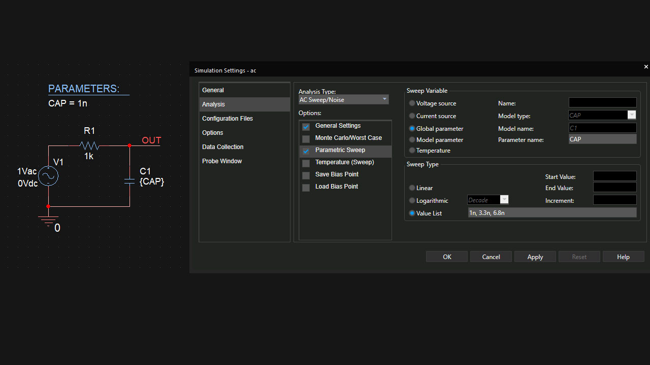
Let's look at an example of this in PSpice for TI. The simulation set up in Figure 1 plots the AC transfer function of a single-pole resistor-capacitor filter network while stepping the value of the capacitor.

PSpice for TI circuit simulation settings showing parametric sweep and AC sweep/noise

Figure 1: PSpice for TI schematic and simulation profile example

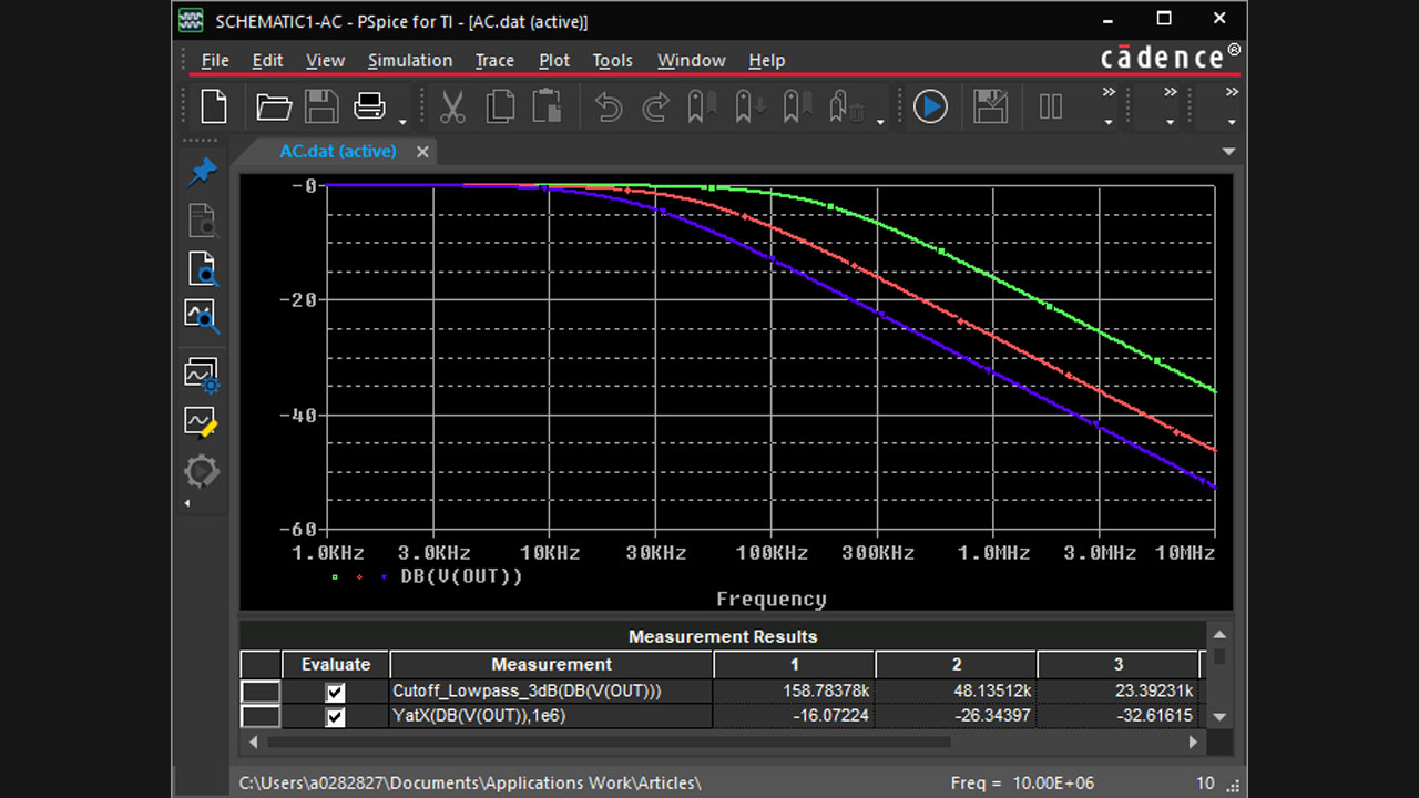
Figure 2 shows the resulting plots, along with automatic measurements of each plot’s -3-dB bandwidth and gain at f = 1 MHz. This powerful analysis capability can greatly expedite design optimization.

 PSpice for TI measurement results for AC sweep

Figure 2: PSpice for TI simulation and measurement results

An important note is that proper simulation results assume the device models are accurate and they converge (which in this context means to arrive at an answer) quickly. Thankfully, TI has some of the most accurate and convergence-friendly models in the semiconductor industry, and is continuously working to develop new models and improve its overall modeling capabilities.

Why use PSpice for TI?

PSpice for TI provides both schematic capture as well as analog circuit simulation. Far from being a limited trial, it harnesses many of the advanced features found in the commercial version of the tool, including automatic measurements and post-processing, as well as Monte Carlo and worst-case analysis. PSpice for TI is built on the latest PSpice release, works when offline, is compatible with projects developed in the commercial version, and offers an unlimited number of nodes and measurements when using TI devices.

Speaking of TI devices, along with a standard suite of component models, the complete library of nearly 6,000 TI analog power and signal-chain models is fully integrated into PSpice for TI, enabling you to add TI parts to your projects with just a few clicks. There’s no need to manually import TI models, and the rapidly growing library will automatically update to stay current with what’s available on TI.com.

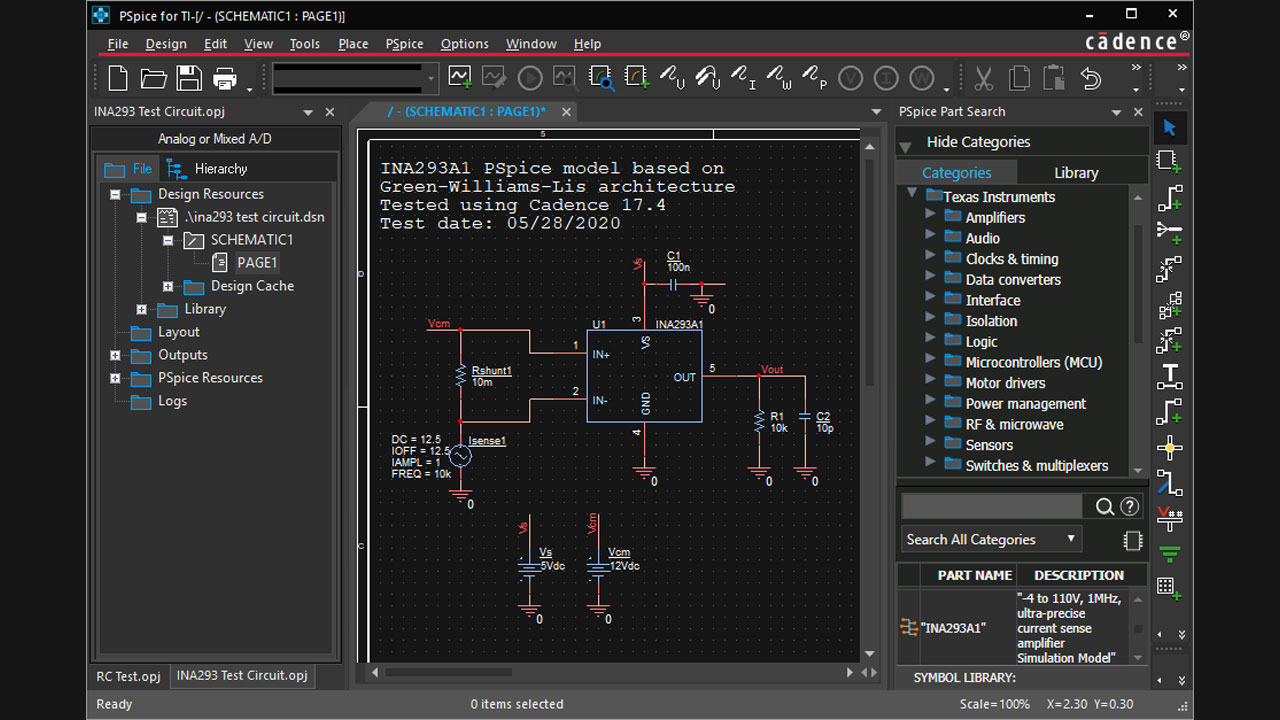
Most TI device models come with a fully tested and operational design example, and in many cases, a complete reference design from which you can cut and paste. This is a great way to quickly get started with a design and rapidly see device operation and performance. You can place a component and open a related reference design with just a few clicks in the tool. Figure 3 shows an example of just one such design example that is ready for modification and simulation. The figure also shows the application’s new dark mode and customizable color scheme, which reduces energy use and may help reduce eye strain. 

INA293A1 PSpice for TI model for circuit simulation

Figure 3: TI device reference design example

To further help you make quicker design decisions, the tool provides easy access to TI product details and data sheets, and relevant queries for support from the TI E2E™ support forums. A library of tutorial videos is also available within the environment.

To add SPICE simulation to your engineering workflow, download PSpice for TI and start reducing your design time, along with the community of engineers already making use of this powerful tool.


Additional resources

  • Find reference designs leveraging the best in TI technology to solve your system-level challenges.
  • Start a new power-supply design with in-depth calculations of voltages and currents using the Power Stage Designer™ software tool.
  • Explore the TI Precision Labs video training curriculum for analog signal-chain design, from foundational knowledge to advanced concepts.
  • Download WEBENCH® Power Designer, a popular, free online power design tool that takes basic input and output specifications and quickly provides a full schematic and bill of materials (BOM).
  • Explore TINA-TI™, a flexible SPICE-based simulation platform that supports a broad range of components, yet maintains a basic user interface sufficient for many analog designs.

eFuses in factory automation: all-in-one system power protection

$
0
0

“All-in-one” sounds so nice, doesn’t it? Nothing encompasses the idea of all-in-one more than the Swiss Army knife, which was first introduced to the world back in 1891 and has become something of a legend given its versatility, small size and low cost. This one tool can help solve a variety of daily challenges and is small enough to fit in your pocket. What more could you ask for?

Now picture a factory floor environment. In this setting, a number of things could go wrong, such as short-circuit events, power interruptions and miswiring events. To avoid these situations, you need to protect your system in order to keep it up and running and prevent factory downtime. Some of the protection functions you may find your programmable logic controller (PLC) or motor drive system needing could include:

  • Field miswiring.
  • Short-circuit protection.
  • Overvoltage protection.
  • Surge immunity.
  • Reverse current blocking.
  • In-rush current control.

Just like the Swiss Army knife, what if there was an ultra-flexible, all-in-one semiconductor device that could provide all of the protection features listed above in a small, affordable design for your 24-V factory automation system?

eFuses from Texas Instruments (TI) are 60-V integrated circuits that provide complete system power protection with just one small component. With a wide operating voltage range (4.5 V to 60 V) suitable for industrial automation applications and high configurability, eFuses are an all-in-one solution for power protection. User-adjustable protection functions on these devices make it easy for you to tweak your design with one small change in resistor or capacitor value – for instance, a current limit or an in-rush current level.

In the past, you may have relied on discrete solutions to protect your system. Discrete solutions can sometimes lead to a bulky and inefficient design, eating into your board space and power dissipation budget. eFuses enable both a small solution size and a lower power dissipation solution. Figure 1 compares a discrete protection circuit and an integrated eFuse circuit for a 24-V/0.8-A input power protection design. The discrete solution and eFuse provide the same functionality, but the eFuse is 81%smaller and 37% more efficient.

Figure 1: Discrete vs. integrated eFuse size comparison

Not only are eFuses highly integrated with a slew of protection features, but they are also affordable – which means that you can use them in any of your designs to reduce your assembly and overall bill-of-materials costs.

Additionally, TI eFuses provide an extensive product life-cycle for your long-life factory automation designs, eliminating the need for constant board revisions to change out components because of end-of-life scenarios with discrete components.

In summary, eFuses offer a compact, ultra-flexible solution to protect your 24-V input from a variety of faults that could occur in a PLC or motor drive system. Robust protection enables your systems to remain operational to reduce factory downtime and increase your operating efficiency.

Additional resources

How to choose a power supply for an automotive camera module

$
0
0

As automotive camera technology advances with higher resolutions, dynamic ranges and frame rates, power-supply architectures need tailoring to the specific use-case requirements. In this article, I’ll review three strategies you can use to power your automotive camera module:

  • Fully discrete
  • Fully integrated
  • Partially integrated

The focus in this article is on small-form-factor camera modules that don’t include any data processing, and output raw video data to a separate electronic control unit. These modules are often found in surround-view, driver-monitoring and mirror-replacement systems and receive a pre-regulated supply voltage over the same coaxial cable used for video data output.

How much power do you need for a camera module?

The first step when designing the power portion of a camera module is a brief calculation of the power budget for each rail. This, along with the voltage provided over power-over-coax (PoC), is important in selecting the power strategy.

A camera sensor and external circuitry require a current draw that may vary widely across different sensors and any additional external devices. Usually, the lower imager rails (1.2 V and 1.8 V in Figure 1) require the most current, while the largest supply voltage (2.9 V for the imager) requires the least. Because the 2.9-V rail pertains to the analog supply of the imager – and ultimately, its performance with regard to image quality – selecting a supply will require careful consideration, as the rail requires a clean supply with minimal noise. The included FPD-Link device, along with any form of supervisors or sequencers, will also pull from this power budget.

­


Figure 1: Calculating the power budget for each rail

One might suggest using a low-dropout regulator (LDO) for every supply considering its excellent noise performance. However, that is not feasible when designing with a limited power budget. Additionally, increasing current will stress connectors and cables and increase self heating of the camera, which may worsen performance.

As shown in the example calculation in Table 1, the current requirements for camera modules are generally determined by the sensor and FPD-Link device included in the system. In this example, the imager rails are 1.2 V, 1.8 V and 2.9 V. The FPD-Link device shares the same 1.8-V rail. The required currents for normal operation are highlighted in red.

Table 1: An example calculation with imager rails at 1.2 V, 1.8 V and 2.9 V

In this example, the PoC supply over the coaxial cable is first stepped down to 3.3 V, which then supplies the rest of the system on the camera module. The 2.9-V sensor analog rail is tied directly to an LDO output, while the other supplies are tied to a step-down (buck) converter. The 1.8-V rail supplies both the DS90UB953-Q1 supply, and the interface supply of the imager. Since the current consumed by the DS90UB953-Q1 serializer is predominantly greater than the imager interface supply, the 1.8-V current provided to the imager can be considered as negligible. The imager 2.9-V analog rail requires 63 mA, the DS90UB953-Q1 serializer 1.8-V rail requires 225 mA and the imager digital 1.2-V rail requires 388 mA. Assuming 100% efficiency to simplify calculations with the previous values, it is calculated that the 3.3-V supply will require 327 mA to successfully power the 1.2-V, 1.8-V, and 2.9-V rails.

Because the input and output voltages, output current requirements, and total wattage consumption are known, the input current can be calculated with:

(PoC Voltage)*(Current required) = 3.3-V * 327 mA

For a PoC Voltage of 12-V, the ECU would source 90 mA.

In some situations, the PoC voltage is fixed from the ECU, therefore it’s important to understand if the chosen PoC cable and network is adequate in supplying the required current for the power goal. For a 2-W camera module requirement, a fixed 5-V supply would source 400 mA, while a 12-V supply would source 166 mA.

For larger PoC cable lengths, a large PoC voltage should be chosen to ensure minimal IR drop across the cable. PoC current will create a voltage drop across the cabling, ferrite beads, inductors, and any series resistance and will reduce voltage headroom impacting camera module regulator performance. In the case that the PoC voltage value is left to the designer, cable specifications generally dictate the amount of current that the network can provide, which will drive the voltage requirement of the network.

Three power architectures for automotive camera modules

Table 2 compares the advantages and disadvantages of the three different power architectures.


Table 2: Comparing camera module power architectures

Supply considerations

When designing for automotive applications, there are a few considerations that will limit your power design choices. Important system-level specifications include:

  • Minimizing the total solution size to meet the small form factor of automotive camera module enclosures. Such enclosures are typically around 20 mm by 20 mm in area and usually fit within an M12 barrel plastic enclosure.
  • Avoiding interference with the AM radio band. All switching power supplies need to be outside the AM radio band of 540 kHz to 1,700 kHz.
  • Avoiding lower switching frequencies because they require large inductors. Instead, choose:
    • High-frequency switchers (>2 MHz).
    • Devices that are Automotive Electronics Council-Q100 rated.
  • Electronics that need added protection such as a short-to-battery can design with wide Vin regulators.

 Printed circuit board constraints

The imager in Figure 2 uses a Mobile Industry Processor Interface (MIPI) Camera Serial Interface (CSI-2), with nets highlighted to display the controlled impedance traces that connect the FPD-Link device to the imager. CSI-2 nets of the imager are brought out through vias and routed mid-layer (highlighted).

The via array poses some limitations to a smaller form factor, as they limit the area of where the power devices can be placed. To minimize coupling, especially around switch-mode power supplies or signal nets, it’s important that CSI-2 nets are properly distanced, shielded and have no overlap from other nets on adjacent layers.

Figure 2: Example layout of the DS90UB953-Q1 with an imager

Choose your power architecture

The right power architecture will vary based on your design requirements. These reference designs will help you see the specifications in greater detail and make your design simpler when you’re ready to get started:

Overcome last-minute requirement changes with SOT-23 multiplexers

$
0
0

We’ve all been there – a late requirement change has thrown your design in disarray, with little time to implement changes and few multiplexer options. There is a myriad of possible last-minute changes, but one that I often encounter when working with designers is how to monitor an increased number of nodes after the microcontroller has already been selected, as shown in Figure 1. One of the biggest challenges in this scenario, ironically enough, is the lack of available board space to fit an additional multiplexer. Fortunately, there’s a relatively easy solution involving small-size 8:1 multiplexers, such as the TMUX1308.


Figure 1: General-purpose input/output (GPIO) expansion with 8:1 multiplexers

When you think small-size multiplexer, you may think your only option is to use a device in a quad flat no-lead (QFN) package. There is another option; however, multiplexers in small-outline transistor (SOT)-23 packaging. Figure 2 shows the size comparison of common 16-pin packages where you will notice the SOT-23 thin is a leaded package that is half the solution size of the thin-shrink small-outline package (TSSOP) used in most designs today.


Figure 2: TI 16-pin package footprint comparison

You can easily replace a 16-pin TSSOP with two 16-pin SOT-23 thin devices and retain the ability to lay them out in a similar area. The SOT-23 thin package also uses a 0.5-mm pitch, which is a widely accepted manufacturing design rule and is easy to hand solder. It offers the size advantage of a QFN and includes leads which are helpful for debugging and prototyping, mechanical reliability, and optical inspection. SOT-23 packages are a good fit if you are trying to increase your board density but your requirements call for leaded packages.


Optimize board space with compromising on performance or cost

 Learn more about the benefits of small-size packaging in the technical white paper, “Designing a Compact Signal Chain for High Performance in Small Spaces.”

SOT-23 multiplexers can also help you handle last-minute requirement changes when you need to add a new system feature late in the design process. Figure 3 shows an example in which the choice of battery monitor circuit was locked, and all GPIOs were being used to measure multiple negative temperature coefficient thermistors (NTCs) around the system. Late in the design, the designer wanted to add a feature that would store battery-life information from the battery monitor in electrically erasable programmable read-only memory (EEPROM).


Figure 3: Battery-management circuit multiplexing between EEPROM and NTCs

In this example, the lead designer was interested in using the SOT-23 package but wasn’t sure if they could get the package qualified as an approved device for their company in time. I suggested that they use a multiplexer like the SN3257-Q1 or TMUX1574, which come in both TSSOP and SOT-23 thin package options. Since the SOT-23 thin footprint can fit inside the TSSOP footprint, as shown in Figure 4, they could place a dual footprint on their printed circuit board (PCB) and mitigate the risk of not having the SOT-23 package approved while continuing forward with the TSSOP package as a backup. Read the Analog Design Journal article, “Second-sourcing options for small-package amplifiers,” for more information on dual-sourcing PCB layouts.


Figure 4: Dual-footprint layout; 16-pin SOT-23 thin footprint inside 16-pin TSSOP footprint

It is inevitable that last-minute challenges will come up when designing a system. Devices historically used to solve these issues now come in smaller package options, so don’t be caught without the tiny leaded SOT-23 thin package. The smaller package options have the size benefit of QFNs and the mechanical benefits of leaded packages. Qualifying the SOT-23 thin package on your approved device list in advance will give you another tool to accommodate last-minute changes on future designs.

How TI helps expand connectivity beyond the front door with Amazon Sidewalk

$
0
0

From lights to locks, homes are becoming more connected – more sensors, more gadgets, more data. As technology continues to advance, consumers crave the ability to monitor, track and sense more, whether it’s temperature, light or motion.

While people’s dependency on technology increases, so does frustration if they’re out of wireless network range, unable to connect, or losing time with network or application installations. Companies developing connected devices often use a variety of wireless protocols, but each protocol works within a certain range and may not talk to other devices.

To help device manufacturers extend the range of their connected devices and enable them to provide a more seamless user experience, TI is now supporting Amazon Sidewalk. Amazon Sidewalk can extend the range of low-bandwidth devices and make it simpler and more convenient for consumers to connect. Ultimately, it will bring more connected devices together into an ecosystem where products such as lights and locks can all communicate on the same network. Sidewalk can enable devices connected inside the home to effortlessly expand throughout the neighborhood.

For example, by utilizing the Sub-1 GHz wireless band (900 MHz), which leverages low data rates to create a long-range, low-power network, Sidewalk will make it possible for consumers to expand their networks into their back yards and stay connected to their other networked devices. This will enable scenarios such as a water sensor that lets you know it’s time to water the garden in the backyard. The extended range can alleviate concerns of dropping connectivity and expands the use cases for connected devices.

To complement the Sub-1 GHz protocol, Amazon Sidewalk also works with Bluetooth® Low Energy to provide greater connectivity around the home.

TI devices supporting the Sidewalk protocol

TI is providing a suite of low-power, multi-band devices with various security enablers to support Amazon Sidewalk. This includes TI’s CC1352R wireless microcontroller (MCU), which supports Sub-1 GHz and Bluetooth Low Energy, the CC1352P wireless MCU, which provides an integrated +20 dBm power amplifier (PA) for an extended range solution, and CC2652P a multi-protocol 2.4GHz wireless MCU with integrated PA. Developers seeking a single-band solution can leverage the CC1312R wireless MCU for 900 MHz or CC2642R wireless MCU for Bluetooth Low Energy. These devices enable developers to build applications that leverage the Sidewalk protocol as well as Bluetooth Low Energy for easy commissioning or over-the-air firmware updates. TI’s Sub-1 GHz devices offer low power FSK (Frequency Shift Keying) modulation technology, which has high spectral efficiency enabling high density low cost applications.

Getting started with your Amazon Sidewalk network

The SimpleLink™ multiband CC1352R wireless MCU LaunchPad™ SensorTag kit (Figure 1) is a Sidewalk-ready development kit that combines integrated environmental and motion sensors with low-power Sub-1 GHz and Bluetooth Low Energy wireless connectivity. With this development kit and TI’s CC1352 software development kit, you can build a Sub-1 GHz or Bluetooth Low Energy application and then in the future leverage Bluetooth Low Energy via a mobile app to load the Sidewalk image.

To stay up to date on the Amazon Sidewalk SDK availability, sign up here. All requests will be vetted and you will be alerted when the software is available.


Figure 1: TI’s LaunchPad Sensor Tag kit 

With the number of connected nodes increasing within homes to the exterior and beyond, the capability to build reliable, long-range networks is critical. Long range connectivity extends our ability to collect more sensor data, monitor more devices and build smarter products. What will you connect next?

Additional resources

How vehicle electrification is evolving voltage board nets

$
0
0

The need for electrical energy inside the car is growing with the proliferation of automated driving functions and the popularity of comfort, convenience and infotainment features. Today’s vehicles have a growing number of sensors, actuators and electronic control modules (ECUs) that read sensors and control actuators. Simultaneously, the growing demand for hybrid and electric vehicles makes power efficiency an important design goal. After all, improved efficiency increases vehicle drive range.

To boost power efficiency, automotive design engineers are implementing higher-voltage board nets in cars. The use of higher-voltage board nets not only helps reduce overall vehicle weight (for example, through reduced harness weight) but also eliminates the need for voltage-level conversion because the higher voltage can directly power the actuator.

Although it may seem that a single high-voltage board net is best, in reality, the varying power requirements of the different actuators and ECUs are leading automotive system designers to implement two to three voltage board nets in vehicles.

In this article, we’ll discuss the voltage board nets that automotive designers are considering in next-generation vehicle architecture. We will also connect you with product families and resources to help you address various technical challenges related to the different board nets.

Figure 1 shows the different voltage board-net possibilities in vehicles based on vehicle type.


Figure 1: Voltage board nets in vehicles

Powering control modules with 12-V board nets

A traditional 12-V board net has a wide voltage range, as prescribed in the International Organization for Standardization (ISO) 7637-2 and ISO 16750-2 standards. While these requirements are unlikely to change for combustion engine-based cars, the use of 12 V in hybrid and electric vehicles could result in a lower maximum voltage, especially if the 12-V bus has no alternator – that is, if all the power needed on the 12-V board net is derived from the high-efficiency DC/DC converter that is used to step down from high voltage to 12 V. In this case, lower-input voltage regulators could be used to implement power-management solutions in ECUs.

Designers have the flexibility to solve different technical challenges in control modules powered by 12-V power board net with a range of automotive-qualified products such as power management, amplifiers, transceivers, motor drivers and smart power switches.

Addressing challenges in 48-V board nets

The 48-V board net is typically used to power loads that require higher power. The specific loads that are powered by 48 V depends on the vehicle type. Regardless of the type of module, control modules connected to the 48 V board net will need power management devices that are efficient, have high power density and are able to withstand operating voltage requirements specified in ISO 21780. The modules also need functional isolation if the ECU is also connected to a 12-V board net. Efficient multiphase 48-V gate drivers with functional safety to drive the 48-V actuators such as the belt starter generator or HVAC AC compressor module. The need for functional safety drives the need for additional diagnostic circuits such as load-current sensing. The deployment of a 48-V power board net would also require efficient, accurate state-of-charge and state-of-health management in 48-V battery-management systems.

To boost efficiency, increase power density and achieve functional safety in 48 V board net systems, designers can use products such as buck regulators, three-phase gate drivers and battery management systems along with the broad portfolio of current and voltage sense amplifiers. 

Maximizing the high-voltage board net

Electric vehicles have battery systems that generate much higher voltage. High power loads such as the traction inverter and the HVAC AC compressor module are directly powered from the high voltage board net. This implies that the power stages that are used to actuate these high voltage loads need to withstand high operating voltages and require high common-mode transient immunity (CMTI). Furthermore, compact solution implementations need high power density gate drivers and power stages. The use of multiple power board nets also requires isolation within the control module between the low- and high-voltage domains to ensure proper operation. The use of high voltage could require designs that not only meet electrical safety requirements but also satisfy functional-safety-requirements. The latter requirements necessitate the implementation of diagnostic features, resulting in additional current-, voltage- and temperature-sensing solution in these systems. Moreover, efficient high voltage battery-management systems that have accurate state-of-charge and state-of-health management and maintain better cell uniformity are also needed.

High voltage gate drivers, battery management systems, power and signal isolators, and high-speed amplifiers are among a broad portfolio of products that designers can use to optimize and meet the challenges of efficiency, power density, functional safety and reliability in high voltage control modules.

Designing  for low to high voltage

Automotive design engineers can choose from a wide range of analog and embedded semiconductor devices for 12-V, 48-V and high voltage board nets. These products offer the flexibility to design vehicle architectures with efficient ECUs and help achieve your power density, reliability and functional safety design goals.

Additional resources:

See our vehicle electrification products and design resources.


The impact of an isolated gate driver’s input stage for motor-drive applications

$
0
0

You have many options when selecting an isolated gate driver for the power stage in motor-drive applications. Gate drivers can be simple or complex, with features such as an integrated Miller clamp, split outputs or an undervoltage (UVLO) lockout reference to the emitter of an insulated gate bipolar transistor (IGBT).

There are two options for input stages: a voltage input stage or current input stage. In this article, I’ll introduce both input stage options and provide a few details you should consider when selecting a gate driver with an input stage for your application.

Voltage input stage

Voltage input devices accept a complementary metal-oxide semiconductor pulse-width modulation (PWM) signal directly into the gate driver on the low-voltage or primary side. Figure 1 shows an example of a typical voltage input isolated gate driver. The input pins, IN+ and IN-, are easy to drive with logic-level control signals available with most microcontrollers (MCUs). Although IN+ and IN- are on the primary side, a voltage gate driver only requires one of the inputs to receive a signal in order to function. Having both IN+ and IN- allows you to configure the PWM input signal as inverting or noninverting.

If you need more noise immunity, you can implement complementary or inverted logic PWM inputs. And if you choose only a single-input pin for your application, you can use the other pin for enable or disable functionality, as described in the application note, “Enable Function with Unused Differential Input.”

Figure 1: Single-channel isolated gate driver with voltage input stage

Current input stage

Current input devices use a current signal into the gate driver on the primary side. Figure 2 shows an example of a typical current input isolated gate driver. These devices are also referred to as optocompatible to match legacy optocouplers. In a legacy optocoupler, a current signal drives an LED inside the device to illuminate when you want the gate driver to turn on. The light emitted by the LED is received by a photodetector. The LED and photodetector are physically separated inside the optocoupler, which creates galvanic isolation from the gate driver’s primary to secondary side.

TI drivers use an emulated diode (e-diode) that helps improve reliability over a gate driver’s lifetime. TI’s optocompatible gate-driver devices use capacitive isolation paired with the e-diode to enable a pin-to-pin solution that is a drop-in upgrade to optical-based gate drivers. The e-diode input stage is not susceptible to effects that can reduce the lifetime of optocoupler gate drivers, such as degradation from higher temperatures or stressing of the input forward current that can both diminish the brightness of an LED. TI optocompatible solutions with the e-diode can help increase system lifetimes in motor-drive applications and operate across a wider ambient temperature range. You can learn more about this topic in the technical article, “Replace your aging optocoupler gate driver.”

Figure 2: Single-channel isolated gate driver with current (optocompatible) input stage

There are system-level differences between voltage and current input gate drivers. A voltage-based solution requires fewer external components, and thus has a smaller total solution size. The MCU can drive voltage-based drivers directly, while current-based drivers need an external buffer to translate the voltage signal from the MCU into a current fed into the gate driver.

Figure 3 compares voltage input and current input gate drivers, as well as the external components required to drive an IGBT. Many designers have traditionally used current input devices to help improve noise immunity for the gate driver. Compared to a voltage signal, current signals are less susceptible to noise such as electromagnetic interference over longer distances. Adding low-pass filters to IN+ and IN- can also help increase the gate driver’s noise immunity and preserve signal integrity.

Figure 3: Comparing voltage input and current input gate drivers

Interlock helps prevent shoot-through in motor-drive power stages, protecting the power switches in high- and low-side configurations. It is possible to achieve interlock with a current input stage gate driver by connecting the anode of the high-side driver to the cathode of the low-side driver, and vice versa. For voltage input stage gate drivers that have a single input, you can implement interlock with external logic components, or connect IN+ of the high-side driver to IN- of the low-side driver (and vice versa) if the gate driver supports both IN+ and IN-. Figure 4 shows a typical interlock example with a current input gate driver.

Figure 4: Interlock example with current input gate driver

TI offers gate drivers for both voltage or current input options, compared below in Table 1.  

TI gate driver family

Input type

Miller clamp

Split output

Emitter-referenced UVLO

Simple single output

UCC23514

Current

UCC23514M

UCC23514S

UCC23514E

UCC23514V

UCC5310

UCC5320

UCC5350

UCC5390

Voltage

UCC5310MC, UCC5350MC

UCC5320SC, UCC5350SB, UCC5390SC

UCC5320EC, UCC5390EC

Table 1: Simple isolated gate drivers with alternative pinout options

A gate driver’s input stage has several implications for your motor-drive application, with system requirements dictating your selection. Whether you need to reduce the total solution size, maximize noise immunity or implement shoot-through protection, TI has many options to help you design your next motor-drive power stage.

Additional resources

Integrating multiple functions within a housekeeping MSP430™ microcontroller

$
0
0

You’re probably constantly looking for ways to optimize your printed circuit board (PCB) designs. From reducing board size to lowering costs and component count, maximizing efficiency is a requirement for almost any design.

Adding a small, low-cost microcontroller (MCU) for simple housekeeping functions can benefit many board designs. This housekeeping (or secondary) MCU is not the main host processor in the system, but it can handle several important system-level functions such as LED control or input/output (I/O) expansion. In this article, I’ll explain how integrating a multifunction housekeeping MCU in your system can help lower bill-of-materials (BOM) costs, save board space, and best of all simplify your design.

For example, let’s say that you wanted to create a new design with these features:

  • LED control
  • I/O expansion
  • External electrically erasable programmable read-only memory (EEPROM)
  • An external watchdog timer

It is possible to use discrete integrated circuits (ICs) to achieve each of these functions. Instead, consider performing all of the functions in software on a housekeeping MCU in order to minimize complexity and reduce board size, as shown in Figure 1.

Figure 1: Implementing the functionality of multiple discrete ICs and in software on a single housekeeping MSP430 MCU


Another design challenge to consider – and perhaps one of the most important – is meeting your design budget.

For instance, looking at the costs associated with a discrete IC approach for these features, you could expect these approximate BOM costs (using web pricing):

In total, a discrete approach to handle housekeeping functions would cost around $0.97. Compare that to the current web price for an 8-KB MSP430 MCU, which is less than $0.25. That’s quite a large savings!

If you require more or less memory for your housekeeping MCU, you can find various options that scale across memory and price in the MSP430 MCU portfolio. Table 1 lists these MCUs and their current TI.com pricing.

Memory

Product

Pricing

 0.5 kB

MSP430FR2000

See Pricing

1 kB

MSP430FR2100

See Pricing

2 kB

MSP430FR2110

See Pricing

4 kB

MSP430FR2111

See Pricing

8 kB

MSP430FR2422

See Pricing

16 kB

MSP430FR2433

See Pricing

Table 1: Housekeeping MSP430 MCUs with TI.com pricing


Not only does an integrated housekeeping MCU approach save board size and reduce the number of components, it also saves BOM costs. You can learn more about these design considerations in the webinar, “Simpler system monitoring: How to offload multiple functions to an MSP430 MCU.


Sample application: Implementing ADC wake and transmit functions on a housekeeping MCU

Let’s walk through an example of how to actually implement the housekeeping function within your design.

One common function is an analog-to-digital converter (ADC) interfacing with other devices on a board for applications such as battery monitors or temperature sensors. In this example, the ADC must periodically sample the analog signals from the sensors and send this data back to the MCU, which will take action based on the behavior of those signals.

If the MCU is using timers to trigger ADC reads, or even receiving ADC values continuously, the system can consume quite a bit of power. One solution is to integrate the ADC into the MCU and operate it independently of the central processing unit (CPU). That way, the rest of the MCU can go to sleep and will only wake up when the ADC reads a value that crosses a certain threshold. At this point, the ADC will generate an interrupt and wake up the MCU.

We describe this application in our training video about housekeeping functions, “ADC Wake and Transmit on Threshold Using MSP430 MCUs.” In this video, we show a graphical user interface (GUI) demonstrating the reading of the ADC values and the sending of the interrupt to wake up the CPU once the threshold is met.

(Please visit the site to view this video)

Conclusion

Using another MCU to perform housekeeping functions is a great way to simplify your design. Plus, with our software and GUI, you can program your MSP430 device in minutes to handle a variety of functions.

Additional resources

How 10BASE-T1L single-pair Ethernet brings the network edge closer with fewer cables

$
0
0

Ethernet is all around us – from points of sale in stores, LED signage in stadiums and even some parts of the industrial automation process. Despite its ubiquity, however, there are areas where it has yet to achieve wide and consistent usage. In this article, I’ll focus on one area in particular, long-distance (>1 km) two-wire networking at 10 Mbps, in remote industrial, building and process automation applications, like the field sensor in Figure 1.


Figure 1: A field sensor that can use 10BASE-T1L Ethernet

There are several reasons why Ethernet hasn’t “reached” these applications yet – most notably that until recently, there wasn’t an Ethernet specification supporting this cable length. Without a defined specification, designers had to use existing Ethernet standards for some parts of network development and other methods for the remainder. But that approach creates several challenges, such as the addition of gateways to support the mix of protocols, which greatly increases system complexity.

There’s also the challenge of cable usage, as standard Ethernet implementations, shown in Figure 2, typically use two to four twisted-pair cables and are not designed for single-pair communications. 


Figure 2: Standard Ethernet interface for 10/100-Mbps communications in a building control application

Because many factory and building automation designers are likely already using existing single-pair fieldbus technologies, such as 4-to 20-mA current loops, Highway Addressable Remote Transducer, (HART) and Control and Communication (CC)-Link for long-distance applications, adding Ethernet to their network through protocol conversion could increase cable cost and weight.

Fortunately, single-pair Ethernet PHYs, especially those for the 10BASE-T1L standard, are designed to help engineers looking to increase the bandwidth of their industrial communications and unify their network under a single interface protocol without increasing cable costs or network complexity.


Transmit 10-Mbps Ethernet signals farther with a single cable

 Meet the DP83TD510E, an Ethernet PHY for the IEEE 802.3cg 10BASE-T1L specification. This device is designed to extend industrial communications up to 1.7 km in process, factory and building automation applications.

What is single-pair Ethernet?

At its most basic level, single-pair Ethernet is Ethernet over a single twisted pair of wires. The standard also enables the coexistence of power and data on a single pair of wires, which is referred to as power over data line.

The overall single-pair Ethernet specification comprises three different categories, shown in Table 1.

Standards

IEEE 802.3cg 10BASE-T1L

IEEE 802.3bw 100BASE-T1

IEEE 802.3bp 1000BASE-T1

Bandwidth

10 Mbps

100 Mbps

1000 Mbps

Cable reach specification

1,000 m (2.4 V p2p); 200 m (1 V p2p)

50 m

15 m

Power dissipation

<110 mW

<220 mW

<600 mW

Communication

Full duplex

Full duplex

Full duplex

Media Access Control interface

Media Independent Interface (MII), Reduced Media Independent Interface (RMII)

MII, RMII, Serial Gigabit Media Independent Interface (SGMII), Reduced Gigabit Media Independent Interface (RGMII)

RGMII, SGMII

Available TI PHYs

DP83TD510

DP83TC811

DP83TG720

Table 1: Single-pair Ethernet category specification requirements and associated TI Ethernet PHYs 

The categories of single-pair Ethernet use the nomenclature “xBASE-T1.” 1-Gbps single-pair Ethernet is 1000BASE-T1, 100 Mbps is 100BASE-T1, and 10 Mbps is 10BASE-T1L or 10BASE-T1S, depending on its implementation. All three versions have a ratified Institute of Electrical and Electronics Engineers (IEEE) 802.3 specification associated with them. Table 1 summarizes the key differences between each category. For the purposes of this discussion, we’ll focus on 10BASE-T1L for longer-distance networking at 10 Mbps.

What are the key benefits of 10BASE-T1L single-pair Ethernet?

In addition to using fewer cables, single-pair Ethernet helps eliminate the need for protocol conversions and other interventions to enable fast, seamless data transfer between operator and edge node. This freedom of data transfer overcomes the challenges mentioned above and supports the large amounts of data needed for enhanced predictive maintenance and system health, safety and throughput.

Expanded connectivity enables the use of Ethernet networking from an app on any internet-connected device to the most remote edge node, such as a field transmitter or building controller, as shown in Figure 3, without sacrificing distance or data rate. In some cases, it’s possible to reuse existing wire harnesses when upgrading from some legacy fieldbus protocols.


Figure 3: Single-pair Ethernet interface for 10-Mbps communications in a building controller

The low-power consumption of 10BASE-T1L single-pair Ethernet physical layers (PHYs) like the DP83TD510 leaves more room in the system power budget for other critical system components. This increased power efficiency matters, since it reduces overall operating costs and can potentially lead to lower carbon emissions. Low power consumption also helps support intrinsic safety implementations defined in the Ethernet Advanced Physical Layer specification by meeting that standard’s external termination scheme. For more information on how the DP83TD510E helps designers extend their network cable reach, see the application note, “Extend Network Reach and Connectivity with IEEE 802.3cg 10BASE-T1L Ethernet PHYs.”

With the development of IEEE 802.3cg, it’s now feasible to transmit data faster and farther over one pair of twisted wires. This innovation enables designers to take Ethernet to the most remote edge node of a network and supports the same network protocol wherever they are located in the world.

Streamlining functional safety certification in automotive and industrial

$
0
0


Functional safety design takes rigor, documentation and time to get it right. Whether you’re designing for the factory floor or the highway, this white paper explains how TI’s approach to designing integrated circuits (ICs) provides you with the resources needed to streamline your functional safety design.

Read the white paper Streamlining functional safety in automotive and industrial. 

Understanding functional safety FIT rate

$
0
0

Functional safety standards like International Electrotechnical Commission (IEC) 615081 and International Organization for Standardization (ISO) 262622 require that semiconductor device manufacturers address both systematic and random hardware failures. Systematic failures are managed and mitigated by following rigorous development processes. Random hardware failures must adhere to specified quantitative metrics to meet hardware safety integrity levels (SILs) or automotive SILs (ASILs). Consequently, systematic failures are excluded from the calculation of random hardware failure metrics.

Read the white paper Understanding functional safety FIT rate.

Optimizing for protection and precision in servo drive control modules with multiplexers

$
0
0
When designing reliable servo drive control modules , both precision and protection are critical for ensuring reliable operation. Underestimating the importance of these features in the design process could lead to incorrect readings or damages to the...(read more)

Keys to quick success using high-speed data converters

$
0
0

Whether you’re designing an aerospace and defense system, test and measurement equipment or automotive lidar analog front end (AFE), hardware designers using modern high-speed data converters face tough challenges with high-frequency inputs, outputs, clock rates and digital interface. Issues might include connecting with your field-programmable gate array (FPGA), being confident that your first design pass will work or determining how to best model the system before building it.

In this article, I’ll take a closer look at each of these challenges.

Rapid system development

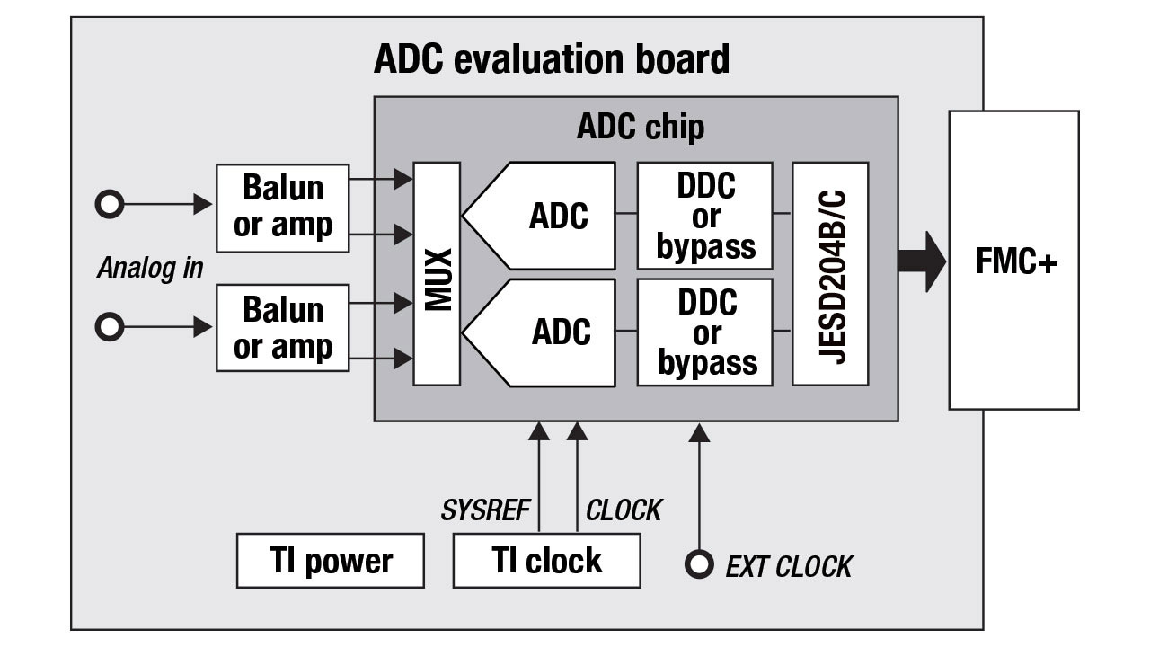
Before starting a new hardware design, engineers often evaluate the most important chips on their own test bench. Once you have obtained the equipment necessary for running the typical evaluation board, component evaluation usually occurs with very idealistic supplies and signal sources. What TI has done in most cases is provide onboard power and clocking so that you can begin running the board with minimal test bench equipment and more realistic power supplies and signal sources, such as the setup shown in Figure 1.

Diagram showing a typical evaluation setup for a high-speed ADC

Figure 1: Typical ADC evaluation board

Once you have validated the performance, you can use the schematics and layout of the more complete evaluation board as a reference design for that portion of the subsystem. Our data-capture and pattern-generation tools support CMOS, LVDS and JESD204, and come with the software needed to operate them. Using the evaluation board user’s guide for your high-speed data converter, it’s possible to get most boards up and running in less than 10 minutes. See Figure 2.

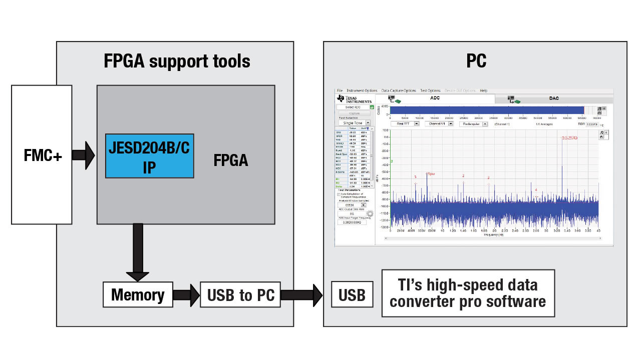
Diagram showing FPGA support tools and ADC data output on a PC. 

Figure 2: TI’s data-capture and pattern-generation hardware and software

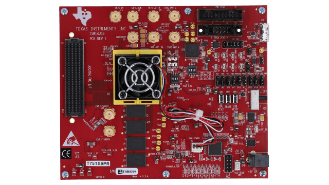
As systems become more complicated, you may need to evaluate across a broader range of use cases. An evaluation board can help. If your evaluation needs become complex, you can use Python, Matlab, Labview or C++ software to directly communicate with the device through the device evaluation board, the capture card solution and the test-bench equipment. Great examples of support boards are the TSW1400EVM for LVDS/CMOS or the TSW14J56EVM for supporting JESD204B serializer-deserializer (SerDes) protocol devices, as shown in Figure 3.

View of a data converter EVM with 8 JESD204B lanes from 0.6-12.5Gbps

Figure 3: TI’s TSW14J56EVM for JESD204B data capture or pattern generation

TI also supports a complete system-level mockup of a multievaluation module prototype from a single PC. For example, it is possible to test transmit-and-receive channels simultaneously by connecting a Xilinx FPGA development kit like the KCU105 or VCU118 to multiple analog-to-digital converters (ADCs) or digital-to-analog converters (DACs).

FPGA connectivity and JESD204B and JESD204C

One of the biggest problems you may have to solve is how to get data to and from your FPGA. While LVDS and CMOS are simple interfaces, they are very limited in the speed they can support per pin on the device. With newer high-speed data converters more commonly supporting input or output rates >1 GSPS, these interfaces either run out of steam or become not-so-simple to design with.

JEDEC, which develops open standards for the microelectronics industry, created JESD204 to solve this problem by supporting differential-pair lane rates beyond 12.5 Gbps. But while JESD204 minimizes the number of pins, it does drive up the interface complexity by encoding and serializing, or deserializing and decoding, parallel data.

Up until now, you have primarily had to rely on JESD204 intellectual property (IP) blocks and support offered by FPGA vendors. While these IP blocks do work very well, they are provided in a manner to support any device in any configuration. This means that they can be difficult to learn and configure for your specific use case. You either have to spend a great amount of effort designing the IP yourself, or seek the IP from a third-party IP provider. However, the third-party IP will require help and support in implementation if things go wrong.

Our JESD204 Rapid Design IP is pre-configurable and optimizable specifically for your FPGA platform, data converter and JESD204 mode. Our IP requires fewer FPGA resources, while also being customized for each particular use. Another benefit is that it takes only hours or days to implement a JESD204 link instead of weeks or months.

Device models

As direct radio-frequency (RF) sampling and extremely fast SerDes become more prevalent in conjunction with high-speed data converters, the ability to model RF and signal integrity is becoming a necessity for first-pass design success. Traditionally, most vendors provide only input impedance information for ADCs in S-parameter models, but our ADC12DJ3200, ADC12DJ5200RF and ADC12QJ1600-Q1 high-frequency input devices, targeted for sampling frequencies up to 8 GHz, now have S-parameter models that include impedance and frequency response information.

With this new model, you can simulate expected device behavior and optimize impedance matching. TI’s strategy is to provide these models on devices supporting very-high input-and-output frequencies, where impedance matching and achieving the desired frequency response are more challenging.

On the digital interface side of the data converter, the Input/Output Buffer Information Specification (IBIS) is a prevalent model that provides physical layer information for CMOS and LVDS pins, as well as DC- and AC-type behaviors. With most new data converters using high-speed JESD204 SerDes, the models have improved to IBIS-Algorithmic Modeling Interface (AMI), which includes information helpful when applying equalization and pre- or post-emphasis. IBIS-AMI provides the modeling you need to get your board right the first time, while achieving a good bit-error rate, signal integrity and robust data link. Figure 4 shows the RF (green) and digital interface (blue) models.

 Diagram of ADC evaluation board, showing RF and interface models.

Figure 4: Modeling the interfaces


Conclusion

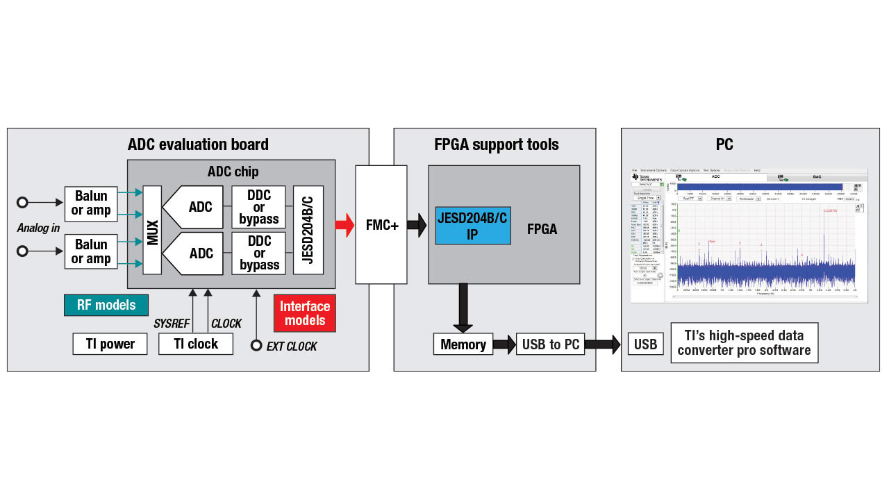
If it’s been a while since you’ve designed with high-speed data converters, or if you’re relatively new to high-speed design, you can take comfort in knowing that TI is making them easier to use. We’ve put together a complete development environment to make all of this easier, shown in figure 5.

With ready-to-use IP for easy FPGA integration, precise RF system models, and the most robust set of flexible, scalable and automatable evaluation modules on the market, you can cut months of firmware development time, reduce costly design cycles and accelerate your high-speed design from concept to prototype.

 Full diagram of ADC evaluation board, RF and interface models, FPGA support tools and PC output.

Figure 5: Typical high-speed analog-to-digital converter (ADC) evaluation environment

Additional resources


How to design an automotive transient and overcurrent protection filter

$
0
0

Somewhere in the world today, an automotive engineer is envisioning an infotainment system for a car that won’t be realized for another five years or more. This includes factoring in the power requirements for applications that exist only as concepts today. As infotainment systems evolve in sophistication and electronic functionality, the number of integrated circuits (ICs) also increases, and the ICs are all sharing power from the 12-V battery.

Designing these power architectures requires the implementation of power conditioning and protection to ensure system functionality across different transient events.

In this article, I’ll review the typical transients that may be of concern, and how TI can help with transient protection needs.


Skip this article, and go straight to the reference design


"Automotive transient and overcurrent protection filter reference design"

Typical transients

Transients can occur in four common scenarios.

Figure 1 depicts the first scenario which is a load dump event caused by the disconnection of the battery from the alternator during battery charging. A load dump event will cause a voltage increase; for a centralized clamp at the alternator, the maximum voltage would be 35 V.

powertrain

Figure 1: Load dump profile for 12-V system

Figure 2 is the second scenario in which a large negative voltage peak (such as International Organization for Standardization [ISO] 7637-2 test pulse 1), which will occur in modules in parallel with an inductive load when a power supply disconnection occurs.


powertrain

Figure 2: ISO 7637-2 test pulse


As shown in Figure 3, the third scenario is inrush current during startup caused by the system’s bulk capacitance, which may lead to higher currents as the capacitors are charging.

infotainment

Figure 3: Inrush current profile during start up with large capacitive loads

The fourth scenario is a decrease in battery voltage. Figure 4 is a cold crank, when the engine starts in a low ambient temperature environment.


infotainment

Figure 4: A typical old crank waveform

Protection against transients

One way to provide transient protection is with an ideal diode controller . As shown in Figure 5, using a current-sense amplifier with an ideal diode controller can provide additional overcurrent protection, resulting in a comprehensive protection solution that precedes any filtering and power conditioning.


infotainment


Figure 5: Automotive transient and overcurrent protection filter protection block diagram

Load dump protection

The LM74810-Q1 provides protection from suppressed load dump events through an adjustable overvoltage feature. As shown in Figure 6, the LM74810-Q1 has an OV pin that uses a comparator to signal an overvoltage event. This will turn off the HGATE voltage that drives the Q2 metal-oxide semiconductor field-effect transistor (MOSFET). Adjusting the resistor-divider connected to the OV pin to your preferred threshold enables the use of lower-voltage-rated components downstream that don’t feature the necessary voltage range needed for possible transients at the input.. The LM74810-Q1 device itself has a maximum input rating of 65 V and should remain operational during a 35-V peak transient event.


infotainment

Figure 6: Typical block diagram of LM74800 with OV protection

Negative voltage transient protection

The LM74810-Q1, along with an appropriate MOSFET and input transient voltage suppression (TVS), protects the system from high negative voltage transients such as ISO 7637-2 test pulse 1. If the input voltage is negative the LM74810-Q1 turns off and causes DGATE to pull low. The body diode of Q1 in Figure 6 will then provide reverse voltage protection to the system and prevent any negative current flow. Once the input voltage returns to its nominal state, the LM74810-Q1 turns back on and enables the MOSFETs for normal operation.

Protecting the LM74810-Q1 during the large negative voltage spike caused by ISO 7637-2 test pulse 1 (typically –100 V or more) requires a TVS diode. The input TVS breakdown voltage should be higher than the 35-V load dump condition but lower than the 65-V maximum voltage rating for the LM74810-Q1. For negative voltages, the TVS diode breakdown voltage should be higher than the voltage seen during a reverse battery connection but low enough such that the negative clamping voltage of the TVS does not exceed the of the Q1 MOSFET.

Inrush current limiting

The LM74810-Q1 includes inrush current-limiting functionality to control current at startup. Depending on the amount of capacitance at the output, this feature limits the current to ensure that components do not experience high current beyond safe operation.

As illustrated in Figure 7, adding a resistor-capacitor (RC) to the HGATE of the LM74810-Q1 slows down the HGATE voltage ramp at startup and thus implements inrush current limiting.

infotainment

Figure 7: Inrush current limiting with LM7480x-Q1


Overcurrent protection

The INA302-Q1 provides overcurrent detection through two independently adjustable threshold comparator outputs. Connecting the active-low comparator output to the enable pin of the LM74810-Q1 allows the MOSFETs to turn off when experiencing an overcurrent condition. The ALERT2 comparator provides the flexibility of having an adjustable delay for the output signal, which may be of use if small current increases may occur during normal operation but you do not want overcurrent protection to trigger during such scenarios. You can adjust the duration of the delay by changing the value of the capacitor placed at the DELAY pin of the device, and adjust the current threshold for the overcurrent event through the INA302-Q1’s ILIM pins; see R5in Figure 8.

infotainment

Figure 8: Implementing an adjustable overvoltage and overcurrent protection

Low-voltage transient protection

Cold-crank and warm-start events can cause low-voltage transients in the system. Negative current may occur from the input being lower than the output during these events and may be of concern for systems that need to maintain functionality. Because the output voltage will decrease as allowed by the output capacitance present, ensuring that current will not flow back to the battery requires reverse current blocking.

The LM74810-Q1 can provide this kind of protection, as it continuously monitors the voltage drop across the Q1 MOSFET between the A and C pins. As shown in Figures 9 and 10, during normal operation the voltage across Q1 will be positive and current can flow to the load. During instances where reverse current may occur – such as when input is lower than the output– the LM74810-Q1 will rapidly respond when the voltage across Q1 reaches –4.5 mV and will turn off the MOSFET, thus preventing DC reverse current. 

infotainment

Figure 9: The LM74810-Q1 monitors the voltage drop across the Q1 MOSFET in order to ensure that DC reverse current does not occur

infotainment

Figure 10: The DGATE that drives the gate of Q1 pulls low when the voltage drop across the MOSFET reaches –4.5 mV, providing reverse current blocking


Flexibility in the harsh automotive environment

With advanced protection of the system at the input, flexibility is awarded to the designer. These protection devices help drive innovation within automotive with expanded opportunity for choices in the rest of the system without worry for functionality or a lack of protection from harsh electrical environments that can be found in a car.

Additionally, a compact two device protection system like the one described here offers a significant reduction in total solution size compared to a discrete implementation. A smaller solution size provides even more space and opportunity for innovation for the rest of the infotainment solution.

Beyond protecting your system, we hope this design helps accelerate your design into the next generation.

See the reference design, "Automotive transient and overcurrent protection filter reference design."

A better automotive display from pixel to picture with local dimming

$
0
0

This article was originally published on eeworldonline.com

Automotive specifications and environmental conditions have caused the automotive display market to lag behind the consumer display industry in contrast ratio, black levels, resolution, curvature and form factor. Automakers are trying to differentiate their infotainment human-machine interface (HMI) displays and catch up to the technological advances now common in smartphone, tablet and television displays.

LCDs now pervade many aspects of modern life and are becoming more prevalent in vehicles, replacing analog and hybrid gauge clusters and becoming standard in the center information display and passenger entertainment areas of the vehicle. However, these displays lack the image quality and contrast ratio that consumers experience with their personal electronics.

If you look at the personal electronics market, you might assume that emissive displays such as organic LEDs (OLEDs) or micro LEDs are the best way to achieve the ideal automotive display. But numerous design and fabrication challenges – including lifetime, cost and peak brightness concerns – have delayed the implementation of OLED displays in automotive systems.

How can automakers meet modern display expectations? A full-array, locally dimmed backlight architecture has the potential to improve the contrast ratio of LCDs to near-OLED levels, while consuming less power than traditional backlight methods.

Lighting LCDs in automotive applications

Automotive displays have traditionally used globally dimmed edge-lit backlight architectures to illuminate through the liquid-crystal and color-filter layers in the thin-field transistor (TFT) LCD panel to generate colored pixels. The liquid crystals allow light to go through or block light from passing to the color filter creating each subpixel. LCD panels with global backlight architectures create light everywhere, regardless of whether the subpixel is on or off, and rely solely on the liquid crystals to block light. The LCD panel’s intrinsic ability to block light will determine the contrast ratio and black levels of the display as shown in Figure 1.

infotainment

Figure 1: The layers within an LCD panel (Source: Meko)

OLEDs in automotive applications

OLEDs and micro LEDs are emissive-based displays, a single pixel is formed by three RGB sub-pixel LEDs. In contrast to TFT LCD panels, emissive displays only generate light where pixels are needed. OLED displays have a greater contrast ratio – as much as 1 million-to-1 – compared to 2,000-to-1 in normal TFT LCD displays. They also have lower peak-illuminance capabilities, however, which are important in automotive displays in order to overcome bright ambient light conditions. The lower contrast ratios and black levels of automotive displays can cause unpleasant nighttime viewing when black cluster and gauge backgrounds and menus produce a gray-hue effect from the LCD light leakage.

Automotive displays are subject to much more environmental variations than their consumer-grade counterparts: whether it’s day, night, hot, cold, or even whether the car bounces up and down as it travels over a rough road. Vehicle displays have strict temperature operating ranges; electromagnetic emission restrictions; and immunity, vibration and lifetime standards. Many of the technological advances in consumer displays fail to overcome these strict environmental requirements. For instance, while many have expected OLED technology to become more widespread in automotive applications for years, it has yet to proliferate due to lifetime, peak brightness and cost concerns.

The case for local dimming

A local-dimming backlight technology is a direct-lit architecture where the LEDs are directly behind the LCD panel as shown in Figure 2. Each LED or zone of LEDs can dim individually to illuminate only those pixels of the display that are needed by dynamically adapting to the image content on the display.

Figure 2: Switching LEDs individually to achieve a better display

A local-dimming backlight technology can help you achieve greater contrast ratios, maintain high peak illuminance, and remain within automotive environmental and cost limits.

The benefits of using a full-array local dimming architecture include:

  • The mitigation of light leakage by dimming the backlight zones where the pixels have darker content.
  • Improved contrast ratios (up to several hundred thousand-to-one) depending on the number of zones, peak brightness and the native contrast ratio of the display.
  • Lower power consumption compared to globally dimmed backlights, since the LEDs are not lit unless needed.

Table 1 compares the benefits and considerations for automotive display options.

Parameter

OLED/micro LED

Full-array local dimming

Edge-lit, globally dimmed backlighting

Contrast ratio

Up to 1 million-to-1

Several hundred thousand-to-1 (depending on the number of zones and the intrinsic panel contrast ratio)

Several thousand-to-1


Brightness

Low peak brightness

Moderate to Good

Good

Other considerations

Low lifetime

Most expensive

Performance is contingent on the number of LEDs and zones; may result in higher costs

Higher LED and LED driver counts

Potential halo effect if too few zones are designed

Cheapest backlight and display solution

Visible light leakage in dark environments

Table 1: A side-by-side comparison of display options.

Designers must be careful when defining the system parameters to ensure that the local dimming performance outweighs the added system cost and artifacts introduced, such as halo effect or module thickness.

To learn more about adopting a local dimming approach in your automotive display, see my article, “Implementing local dimming into an automotive display,” or check out Automotive 144-Zone Local Dimming Backlight Reference Design. By improving the contrast ratio of traditional edge-lit LCD displays, full-array local dimming in automotive displays could bridge the gap in display performance.

Pixel perfect automotive display: higher contrast and better resolution with full-array local dimming

$
0
0

This article was originally published on eeworldonline.com

A local dimming backlight technology individually adjusts LEDs in an LCD panel to save power and improve contrast ratios in automotive displays. Compared to globally dimmed displays and organic LEDs (OLEDs), local dimming with LEDs is a more practical design choice because it can withstand the extreme temperatures and vibration common in automotive applications and offers better performance than globally dimmed displays.

It is possible to achieve peak performance from a full-array local dimming architecture with a delicate approach toward the optimal number of LEDs and zones. In this article, I’ll review some of the design considerations for implementing such an architecture.


Read part one,“A better automotive display from pixel to picture with local dimming”


Check it out

Design considerations for implementing local dimming

System cost and performance of a local dimming system are directly related to the number of LEDs and zones. If there are too few zones, the resulting zone size will be too large, and a halo effect will occur where light bleeds into pixels that need to be fully dark for the best contrast. Other causes of the halo effect include a light spread function of the particular zone, zone overlap, spatial filters in the dimming algorithm, and the native contrast ratio of the LCD panel.

To achieve the native contrast ratios required for undetectable halo-effect levels comparable to OLEDs, one study concluded that an LCD with a 5,000-to-1 contrast ratio requires 200 local dimming zones, while a 2,000-to-1 contrast ratio requires over 3,000 local dimming zones.

Figures 1 and 2 demonstrate the undesirable illumination of black pixels surrounding white pixels. The left half shows the higher black levels realized by local dimming and the halo artifact introduces immediately surrounding the white box. The right half shows a traditional edge-lit LCD with no halo effect but with a lower contrast ratio due to the light leakage of the LCD.

Figures 1 and 2 compare the halo effect with local dimming (a); and a traditional edge-lit LCD (b)

Careful consideration needs to be taken during the definition of the local dimming system parameters to ensure that local dimming performance outweighs the added system cost and artifacts introduced. The thickness of the backlight module, halo effect, thermals and system cost are all trade-offs to consider.

The number of dimming zones and LEDs per zone are the main priorities when designing a local dimming system. This combination defines the pitch of the LED array, which impacts the backlight module’s overall thickness to achieve homogenous light distribution across the display. In addition to optical layers, such as diffusers and polarizers, increasing the air gap between the LEDs and panel glass will better distribute the light evenly through the panel. The number of dimming zones is directly proportional to the amount of halo artifact created by the system, as more zones will better match the display’s pixels and reduce the unwanted illumination of dark pixels.

Components of an automotive display local dimming system

An automotive local dimming backlight module and LCD display system have similar but slightly modified components when compared to a traditional globally dimmed backlight system. The major components include a timing controller (TCON), LED drivers and LED backlight unit, as shown in Figure 3.

The TCON will convert a video input, such as Open Low-Voltage Differential Signaling (LVDS) interface, LVDS or Red-Green-Blue, into control signals for the source and row drivers in the LCD panel. In a local dimming system, the TCON is specialized to include the internal processing and histogram calculations for the individual zone dimming, with a Serial Peripheral Interface output to control the LED drivers.

Traditional edge-lit backlight units contain 20 to 80 LEDs along the edge in conjunction with light guides, diffusers and polarizers. The locally dimmed LED backlight unit will contain anywhere from 96 to as many as 1,000 LEDs or more uniformly dispersed in a grid, directly behind the LCD to be illuminated. The LEDs are all individually (or sometimes grouped together as two or four LEDs in series or in parallel) controlled by a single low-side channel from the LED driver.

Instead of the single four- to six-channel low-side LED driver used in edge-lit architectures, a local dimming architecture uses multiple 16- to 48-channel LED drivers to achieve the higher zone counts. Multiple LED drivers can have the control signals daisy-chained together to provide an easily controlled and scalable approach based on the number of zones needed.

Figure 3: The components of a local dimming system for automotive displays

Table 1 compares OLED, local dimming and traditional edge-lit globally dimmed backlight implementations.


Table 1: A comparison of display lighting options.

Full-array local dimming in automotive displays could bridge the gap in performance displays in the consumer market. Local dimming improves the contrast ratio of traditional edge-lit LCD displays that underperform due to their low native contrast ratio and light leakage.

The key takeaway for designing a local dimming system for an automotive display is to choose the right number of LEDs spread across the right number of zones. To see more technical information and a demonstration of the local dimming backlight architecture, check out, utomotive 144-Zone Local Dimming Backlight Reference Design


How many electric motors are in your car?

$
0
0

The U.K., Norway, the Netherlands, Denmark and France have already proposed plans to outlaw internal combustion engines (ICE), with China also studying when to ban ICE vehicles. So the writing is on the wall that powerful electric motors, also known as traction motors, will play a significant and increasing role as the engine propelling the vehicle. But electric motors are already dominant in many other automotive applications. Let’s take a motor census of the typical automobile.

infotainment

Figure 1: Electric motor applications in an automobile

Existing – and increasing – motor populations
Electric starter motors have been part of automobiles since your great-grandparents decided there had to be a better way than a hand-crank to start the car. Starter motors are still typically the most powerful electric motors other than traction motors. With the advent of start-stop technology and mild hybrid vehicles, the starter motor is morphing into the starter-generator, and taking on more functions. In some designs, an enhanced starter motor can be used to “creep” forward in stop-and-go traffic, blurring the lines between a starter motor and an electric traction motor.

Windshield wipers are perhaps the most prevalent example of electric motors in existing automobiles. Every car has at least one wiper motor for the front wipers. The popularity of SUVs and hatchbacks with less-streamlined back windows has meant the presence of rear wipers and corresponding motors on a large fraction of cars as well. Another motor pumps washer fluid to the windshields, and in some cars to the headlights, which may have their own small wipers.

Just about every car has blower fans that circulate air from the heating and cooling system; many vehicles have two or more fans in the cabin. High-end vehicles have fans built into the seats for cushion ventilation and heat distribution.

Power seats are fertile ground if you’re looking for electric motors. In economy cars, motors provide convenient front and back adjustment and back cushion tilt. In premium cars, electric motors control options like height adjustment, bottom cushion tilt, lumbar support, headrest adjustment and cushion firmness. Other seat functions that use electric motors include power-seat folding and power stowage of back seats.

Windows used to crank up by hand, but now power windows are common; future generations won’t understand the traditional circular hand motion to ask someone to lower their windows.

Each window is another potential location for an electric motor, including variants such as sunroofs and rear-vent windows in minivans. The drives for these windows can be as simple as a relay, but safety requirements such as detecting an obstacle or pinched object lead to more intelligent drive options, with motion monitoring and limits on drive force.

Locks are another convenience option where manual operation has given way to an electric motor drive. The advantages of electrical control include convenience features such as remote operation, enhanced security and intelligent functions, such as automatic unlock after a collision. Unlike power windows, power door locks must retain the option of manual operation, so this impacts the design of the electric door lock motor and mechanism.

Indicators on the instrument panel, or cluster may evolve to light-emitting diodes (LEDs) or other types of displays, but for now, each dial and gauge uses a small electric motor. Other electric motors in the convenience category include common features like side mirror fold and position adjustment, as well as more exotic applications like convertible roofs, extendable running boards, and glass partitions between the driver and passengers.

Under the hood, electric motors are becoming more common in several places. In most cases, electric motors are replacing belt-driven mechanical components. Examples include radiator fans, fuel pumps, water pumps and compressors. Moving these functions from a belt drive to an electric drive has several advantages. One is that driving electric motors with modern electronics can be much more power-efficient than using belts and pulleys, leading to benefits like higher fuel efficiency, reduced weight and lower emissions. Another advantage is that using electric motors rather than belts allows freedom in mechanical design, as the mounting position of pumps and fans need not be constrained by having to run a serpentine belt to each pulley.

Technology trends
Most electric motors in today’s cars run from the standard 12-V automotive system, with a belt-driven alternator to generate voltage and a lead-acid battery for storage. This arrangement has worked fine for decades, but the latest vehicles need more and more current for comfort, entertainment, navigation, driver assistance and safety features.

A dual-voltage 12-V and 48-V system could move some of the higher-current loads off the 12V battery. The advantages of using a 48-V supply are a 4x reduction in current for the same power, and an accompanying reduction in weight in terms of cables and motor windings. Examples of high-current loads that may migrate to a 48-V supply include the starter motor, turbocharger, fuel pump, water pump and cooling fans. Implementing a 48-V electrical system for these components could result in fuel-consumption savings of around 10%.


How vehicle electrification is evolving voltage board nets


See the technical article and infographic

Brushed DC motors are the traditional solution for driving most electric convenience features in an automotive body. Since the brushes provide the commutation, these motors are simple to drive and are relatively inexpensive. In some applications, brushless DC (BLDC) motors can provide significant benefits in terms of power density, thus reducing weight and providing better fuel economy and lower emissions. Manufacturers are using BLDC motors in windshield wipers, cabin heating, ventilation and air-conditioning (HVAC) blowers and pumps. In these applications, the motor tends to run for long periods, as opposed to momentary operation such as in power windows or power seats, where the simplicity and cost-effectiveness of brushed motors still hold an advantage.

So how many electric motors are in your car?
You would be hard-pressed to find a late-model car with less than a dozen electric motors, while typical modern cars on American roads might easily have 40 electric motors or more. The increasing popularity of electric vehicles will spur many innovations in automotive electric motors. However, electric motors are already prevalent throughout ICE-propelled vehicles, with more applications in each successive model year bringing more convenience, better intelligence and safer operation while reducing environmental impact. Still – there is always room for more.

Minimize noise and ripple with a low-noise buck converter

$
0
0

Minimizing noise is a common challenge for engineers designing a power supply for noise-sensitive systems for test and measurement and radio applications, such as clocks, data converters or amplifiers. Although the term “noise” can mean different things to different people, in this article I’ll define noise as low-frequency thermal noise generated by resistors and transistors in the circuit. You can identify noise through a spectral noise-density curve in microvolts per square-root hertz, and as integrated output noise in root-mean-square microvolts, typically over a specific range from 100 Hz to 100 kHz. Noise in the power supply can degrade the analog-to-digital converter’s performance and introduce clock jitter.

The traditional setup for powering a clock, data converter or amplifier is to use a DC/DC converter, followed by a low-dropout regulator (LDO) such as the TPS7A52, TPS7A53 or TPS7A54, followed by a ferrite-bead filter, as shown in Figure 1. This design approach minimizes both noise and ripple from the power supply and works well for load currents below approximately 2 A. As loads increase, however, the power loss in the LDO introduces issues in efficiency and thermal management; for example, a post-regulation LDO can add 1.5 W of power loss in a typical analog front-end application. Are those of you looking for low noise and efficiency in your design out of options? Not quite.

Figure 1: A typical low-noise architecture using a DC/DC converter, LDO and ferrite-bead filter

Using a low-noise buck converter in place of an LDO

One way to keep the power loss in check is to minimize the dropout through the LDO. However, this approach will have a negative impact on noise performance. Additionally, higher-current LDOs are typically larger, which can increase design footprints and cost. A more effective way to ensure low noise while controlling the power loss is to eliminate the LDO from the design altogether and use a low-noise DC/DC buck converter, as shown in Figure 2.

Figure 2: Using a low-noise buck converter without an LDO

I know what you’re thinking: How does removing the primary device that reduces noise still provide a low-noise supply? Many LDOs have a low-pass filter on the bandgap reference to minimize the noise into the error amplifier. The TPS62912 and TPS62913 family of low-noise buck converters implement a noise-reduction/soft-start pin for connecting a capacitor, forming a low-pass resistor-capacitor filter using the integrated Rf and externally connectedCNR/SS, as shown in Figure 3. This implementation essentially mimics the behavior of the bandgap low-pass filter in an LDO. 

Figure 3: Low-noise buck block diagram with bandgap noise filtering

What about the output voltage ripple?

Every DC/DC converter generates an output voltage ripple at its switching frequency. Noise-sensitive analog rails in precision systems need the lowest supply voltage ripple to minimize frequency spurs in the spectrum, which typically depend on the switching frequency of the DC/DC converter, inductor value, output capacitance, equivalent series resistance and equivalent series inductance. To mitigate the ripple from these components, engineers often use an LDO and/or a small ferrite bead and capacitors to create a pi filter to minimize ripple at the load. A low-ripple buck converter such as the TPS62912 and TPS62913 leverage this ferrite-bead filter by integrating ferrite-bead compensation and remote-sense feedback. Using the inductance of the ferrite bead in combination with an additional output capacitor removes the high-frequency components in the output voltage ripple and reduces the ripple by approximately 30 dB, as shown in Figure 4. 

Figure 4: Output voltage ripple before the ferrite-bead filter (a); and after the ferrite-bead filter (b)

Conclusion

By integrating features that mitigate system noise and ripple, low-noise buck converters can help engineers achieve a low-noise power-supply solution without the need for an LDO. Of course, the noise levels required by different applications will vary, as will the performance for different output voltages, so only you can determine the best low-noise architecture for your design. But if you’re looking to simplify the design of noise-sensitive analog power supplies, reduce power losses, and shrink the overall design footprint, consider using a low-noise buck converter.

Additional resources

Viewing all 4543 articles
Browse latest View live


<script src="https://jsc.adskeeper.com/r/s/rssing.com.1596347.js" async> </script>