Quantcast
Channel: TI E2E support forums
Viewing all 4543 articles
Browse latest View live

How to select the right digital isolator for your design

$
0
0

With the growing popularity of digital isolators in industrial and automotive applications, it can be overwhelming to select the best device for your system from the plethora of available options. Adding to this challenge, most digital isolators are designed with specific system requirements and applications in mind, leaving you to sort through endless specifications and features to ensure that the device you have selected will meet your system’s requirements.

Finding the “right” device doesn’t have to be complicated, however. In this article, I’ll walk through some of the primary decisions for selecting a digital isolator that I hope will help simplify your search.

Step one: understanding your isolation specification requirements

The first step is to understand your system’s isolation specification requirements. While requirements can sometimes feel like an open-ended list, to get started, consider these requirements related to common isolation design:

  • Isolation withstand voltage (VISO). Is basic isolation and ≤3,000 VRMS sufficient for your design, or do you require ≥5,000 VRMS? Regulatory requirements often dictate this specification, which represents the voltage the isolator can handle without breakdown for at least 60 s.
  • Working voltage (VIOWM). What is the consistent voltage that your isolation barrier needs to withstand for the lifetime of the product? Factors such as package size, pollution degree and material group can affect the working voltage of a component.
  • Surge isolation rating(VIOSM). Does the design require reinforced isolation? If so, you will need an isolator that can withstand >10-kV surge pulses.
  • Creepage/clearance. Is 4-mm creepage/clearance sufficient, or does your system standard require 8 mm or even higher? This specification will be dictated by the isolators package and lead frame. 
  • Common-mode transient immunity (CMTI). Will the system be in a noisy environment such as motor drives or solar inverters, where data integrity is critical and any bit errors can result in dangerous short-circuit events? If so, a high CMTI rating will be critical for your digital isolator.
  • Power consumption. Is overall system power consumption a critical specification for your application; for example, is the system 4- to 20-mA loop-powered or battery-powered? If so, consider the per-channel current consumption specifications of each device.
  • Data rate. What data rate does your communication interface require? Are you running slow universal asynchronous receiver transmitter speeds or high-speed ≥100-Mbps data protocols? In that case, you may consider each devices' maximum data rate.

Step two: selecting the right package

Once you have narrowed down your digital isolator specification requirements, the next step is to consider different package options. Packages can make a big difference when it comes to isolation, since the size and characteristics of the package directly affect a device’s high-voltage capabilities. Some of the same requirements in the list above (creepage, clearance, VIOWM, VIOSM, VISO) also influence package selection. A larger package with wider creepage and clearance will allow for higher isolation voltage specifications. If you can meet your system’s regulatory requirements with a smaller package option, a smaller package will of course help save both board space and cost. Additionally, you will want to consider how many channels of isolation your communication interface requires since higher channel counts dictate package type.

You can learn more about creepage and clearance and their effect on isolation in the TI Precision Labs video, “1.6 TI Precision Labs – Isolation: What are Creepage and Clearance?

Step three: determining channel count and configuration

After specifications and requirements and packaging, there are just a few more options to consider. Determining how many channels of isolation you need for your signals and which direction each signal will go will help you determine your channel count and channel configuration. And considering your preferred default output state (or fail-safe state) will help you determine the predefined state of the output pin (either high or low) when the input channel of a digital isolator is unpowered or the pins are left floating. Options may be available for both default-high and default-low outputs.

Step four: assessing available devices

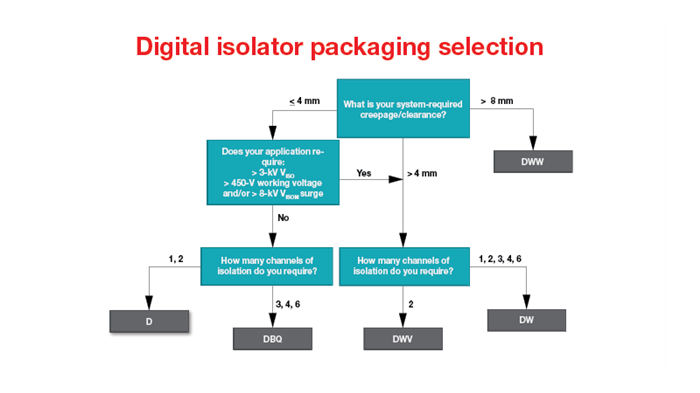
If you’re ready to put your digital isolator knowledge into practice, Figure 1 is a simple digital isolator selection flowchart that can help you determine the right device for your design. Figure 2 can help guide you to the right package designator and Figure 3 shows each package to scale, side by side.

Figure 1: TI digital isolator selection flowchart


Use this list to learn more about the devices in the TI digital isolator selection flowchart:

  • ISO67xx: Basic and reinforced isolation for cost-sensitive applications.
  • ISO77xx: Basic and reinforced digital isolators.
  • ISO78xx: Highest isolation rating, widest creepage/clearance, reinforced digital isolators.
  • ISO70xx: Ultra-low power digital isolators.
  • ISO73xx: Low-power, low-jitter digital isolators.
  • ISO76xx: High-speed, 150-Mbps isolation. 

Flowchart that overviews available packaging options for digital isolators

Figure 2: TI digital isolator package type selection flowchart


Figure 3: Comparison of available package options

Conclusion

There are many options when it comes to digital isolator products. Understanding your system and design requirements and leveraging the resources in this article will help you select the best digital isolator for your design. Selecting the “right” device could optimize your system’s overall design - helping you more easily meet regulatory requirements and your ability to develop reliable applications while staying within budget.

Additional resources


5 myths shattered about 48-V systems

$
0
0

Technology availability, market and environmental regulations, and infrastructure buildout are aligning to turn a long-forecasted future of full-electric vehicles (EVs) into reality. According to the International Energy Agency’s Global EV Outlook 2020, sales of EVs, including plug-in hybrid electric vehicles (PHEVs), reached a global peak of 2.1 million in 2019, increasing the total number of such vehicles on the road to 7.2 million. 

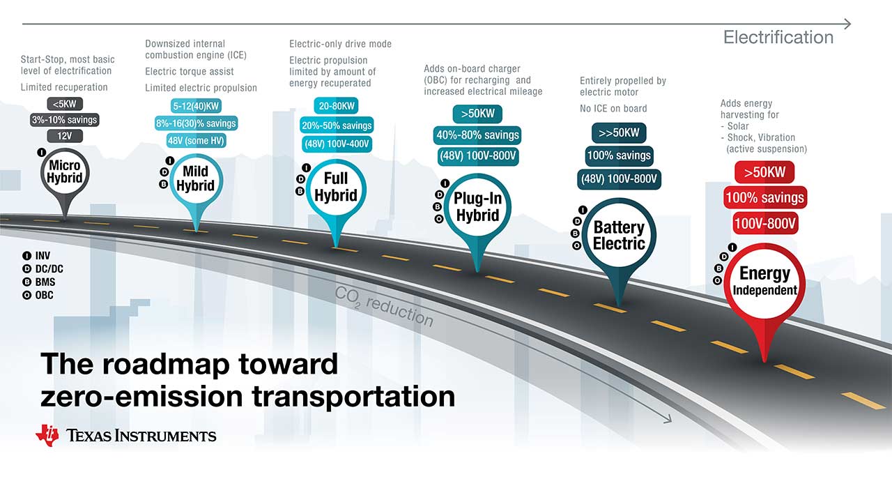
However, even with 40% year-on-year growth, EVs represent a mere 1% of the global car market and 2.6% of global car sales, with internal combustion engine (ICE) vehicles comprising the balance. The need to reduce carbon-dioxide (CO2) emissions and comply with government regulations is pushing automakers to introduce 48-V mild-hybrid (MHEV) models. The range from hybrid to electric to energy independent is depicted in Figure 1. 

powertrain

Yet misconceptions and well-meaning loyalties to fully electric drivetrains persist. In this article, I’ll address five myths about MHEVs. 

Myth No. 1: The market cannot take any more segmentation with 48-V MHEVs.

The market already offers a variety of ICE alternatives in plug-in HEVs and battery EVs (BEVs) even when not all consumers are ready to give up ICE vehicles. Deloitte’s 2020 Global Automotive Consumer Study indicates that 10% of potential buyers in India and 43% of auto buyers in Germany are not willing to pay more for an EV. 48-V MHEVs are less likely to further fragment the market than they are to fulfill existing demand by addressing both range anxiety and cost concerns, and edge consumers closer to the electric future. 

Myth No. 2: OEMs will skip 48 V in their move toward EVs.

In their report, “Reboost: A Comprehensive View on the Changing Powertrain Component Market and How Suppliers Can Succeed,” consultants McKinsey & Co. estimated the need for a cumulative $50 billion investment in the EV charging infrastructure by 2030 (not including grid upgrades) to support the current growth trajectory of the plug-in HEV and battery-powered EV market. Most original equipment manufacturers (OEMs) are embracing 48-V systems because they require merely a step-change in vehicle architecture, whereas combustion-engine cars need expensive redesigns to become battery-powered EVs. 

48-V systems are gaining popularity at a time when the number of electrical subsystems is increasing, thus increasing the need for more power, along with greater environmental concerns and regulatory compliance pressures. 

With automotive suppliers expanding their MHEV portfolios, a growing number of OEMs have planned or launched MHEVs. 

Myth No. 3: 48-V systems will make cars more expensive.

Despite the higher cost of new components, including the additional battery, there are savings elsewhere, including:

  • A size and weight reduction in nearly 4 km of cabling and in wire harnesses because 48 V allows for smaller wire gage than that possible with 12 V.
  • Reduction in costs due to better efficiencies achieved with 48 V electric pumps, fans, power-steering racks and compressors.
  • Reduction in battery cost due to lower requirements compared with those from PHEVs and BEVs.
  • Downsizing potential; for example, replacing a six-cylinder engine with a smaller, lower-cost four-cylinder engine while maintaining performance. 

Moreover, it is possible to manage MHEV costs through design – from the lowest-cost P0 architectures, which run off the accessory belt, to tightly integrated P4 architectures, where electric motors apply torque directly to the axle. 

While economies of scale can further offset upfront costs, MHEVs also lower the true cost to own by improving fuel efficiency, with features such as longer engine-off time during start/stop events, energy capture via recuperative or regenerative braking, and torque assist for the ICE engine. 

Myth No. 4: 48-V systems will replace 12-V systems.

MHEVs are likely to continue linking a conventional 12-V battery to the 48-V system through a DC/DC converter. In current designs, the 48-V system handles loads from climate control and torque assist and helps reduce startup times, while the 12-V system continues controlling the engine, controls the transmission, and handles active safety and infotainment functions, which minimizes redesign and the related costs.

Eventually, high-end vehicle manufacturers will switch to 48-V systems completely, but this will likely take 10 to 15 years. 

Myth No. 5: The world needs full EVs now.

Actually, the world needs to reduce CO2 emissions now, and regulations are finally beginning to effect change toward this goal. In 2021, the European Union will begin limiting CO2 emissions to 95 g/km, with plans to further limit them to 59 g/km or more by 2030. Countries including China, India, Canada and the U.K. have also announced targets to phase out ICE vehicles over the next couple of decades.

Although EVs are available for consumers willing and able to make the switch today, MHEVs offer a path of increasing electrification of transportation. It is a path that helps address concerns about cost, range, and the environment while continuing to utilize both the existing economies of scale and customer expectations. Many carmakers and OEMs now have significant as well as growing 48V product portfolios.

Wherever you are on this path, whether you are designing an MHEV or an EV, we can help you at any level.

Additional resources

How analog integration simplifies automotive body motor controller designs

$
0
0

Automotive body electronics systems use electric motors to enhance comfort and convenience for vehicle occupants whether it’s adjusting the perfect seat position or easily opening the trunk.
Metal-oxide semiconductor field-effect transistors (MOSFETs) – arranged in the shape of the letter “H” – control the electric motors for these applications. But using MOSFETs as switches presents new technical challenges in electronic control module designs, including electromagnetic interference (EMI) and thermal management, current sensing, power-off braking, and diagnostics and protection. The integrated circuit (IC) motor driver products developed by Texas Instruments integrate analog features that help electronic control module designers overcome these challenges while reducing solution size and shortening development times.
 
In this article, we will discuss specific analog features integrated into motor drivers ICs that help address these design challenges

Mitigating EMI
EMI mitigation is achieved using features and solutions both at IC level and at printed circuit-board (PCB) level. One key method to mitigate to EMI is control of pulse width modulation (PWM) edge rates. Gate driver products such as  DRV8705-Q1, DRV8706-Q1, DRV8714-Q1 and DRV8718-Q1 gate drivers for brushed DC (BDC) motors, and three-phase DRV8343-Q1 for brushless DC (BLDC) motors all integrate smart gate-drive technology, which is specifically used to control the PWM edge slew rates. Furthermore, these devices offer the ability to select slew rate that best mitigates EMI. Another common technique used to reduce EMI is dithering the main clock frequency. DRV10983-Q1 three-phase  BLDC motor driver with integrated MOSFETs also integrates dithering of the main clock frequency, thus reducing the amplitude by spreading the peak across the spectrum

Managing thermals
Motor operating and stall currents have a wide range of values based on the load being driven. For high current loads, gate-driver products give you the choice of implementing your designs using discrete MOSFETs. Electronic control module designers can optimize layout and thus achieve optimal thermal management. For low load current loads, devices such as DRV8873-Q1, DRV8874-Q1 and DRV8876-Q1 with integrated H-bridge MOSFETs can be used to drive the loads while achieving optimal thermal management.  Moreover, for low current loads driven by three-phase BLDC motors, DRV10983-Q1with integrated MOSFETs can be used. Note that DRV10983-Q1 also integrates the commutation algorithm, enabling single-chip solution to drive the motor.

Current sensing
The current in the motor is measured to detect circuit and motor faults,. and to infer motor position using ripple counting. All TI BDC and BLDC motor- and gate-driver products integratecurrent-sense amplifiers to amplify the voltage across the resistor. Furthermore, the DRV8106-Q1, DRV8706-Q1, DRV8714-Q1 and DRV8718-Q1 offer an in-line current-sense amplifier. Using in-line current sense measurements, the direction of motor rotation can also be determined.
Windows are traditionally driven using BDC motors. However, system designers are investigating the use of BLDC motors to drive the window because BLDC motors are quieter. In addition, BLDC motors are also being considered for rotating the seat base in autonomous vehicles. The 3-phase smart gate driver DRV8343-Q1 which integrates the current sense function can be used in these applications.

Power-off braking
With MOSFET solutions, a motor can be rotated freely when power to the motor is turned off. In such cases, moving the load manually, for example, opening or closing a power trunk manually, could result in large back EMF which could damage the electronics. The DRV8714-Q1 and DRV8718-Q1, targeted for trunk control module applications, integrate a power-off braking feature, which measures the voltage being generated and applies electronic brakes to the motor. This feature stops the motor from rotating, which in turn stops the generation of current.

Diagnostics and protection
Detecting circuit faults and protecting the systems against these faults is an important requirement when controlling motors. The BDC and BLDC gate drivers integrate diagnostic circuits to detect open and short circuits. In addition, we also provide failure-mode distribution and pin failure mode analysis information for some ICs to aid functional safety design when needed.

Implementing control modules in body applications
Table 1 maps the products to the motors used in these applications.
Control module
Load
Products
Single window with BDC motor
DRV8705-Q1, DRV8706-Q1
 
Door lock motor
Dual window with BDC motor
DRV8714-Q1, DRV8718-Q1, DRV8873-Q1
 
Single window with BLDC motor
DRV8343-Q1
 
Mirror X/Y motor
Mirror fold motor
DRV8908-Q1, DRV8873-Q1
Roof motor
DRV8705-Q1, DRV8706-Q1
 
Multiple roof motor
DRV8714-Q1, DRV8718-Q1
Single trunk lift BDC motor
DRV8705-Q1, DRV8706-Q1
 
Multiple trunk lift BDC motors
DRV8714-Q1, DRV8718-Q1
 
Single trunk lift BLDC motor
DRV8343-Q1
 
Trunk cinch motor
DRV8873-Q1
Seat position adjust motor
DRV8718-Q1, DRV8714-Q1
 
Lumbar support bladder pump motor
DRV8873-Q1, DRV8874-Q1
 
Seat ventilation motor
DRV10983-Q1
 
Seat base rotation motor
DRV8343-Q1
 
Table 1: A selection of products available for body motor applications

Additional resources:

Simplify your isolated current and voltage sensing designs with single-supply isolated amplifiers and ADCs

$
0
0

It is necessary everywhere – to protect humans, provide noise immunity and handle ground potential differences between subsystems. You design for it in applications such as motor drives, solar inverters, DC charging (pile) stations, industrial robots, uninterruptible power supplies, traction inverters, onboard chargers and DC/DC converters.

I’m referring, of course, to galvanic isolation.

Systems, like the ones I mentioned above, require the transfer of current and voltage information from one power domain to the other over an isolation barrier for monitoring and control purposes. How do you transfer analog information over the isolation barrier? The answer lies in isolated amplifiers and isolated analog-to-digital converters (ADCs), the latter of which are also known as isolated delta-sigma modulators.

One key challenge when designing these systems is figuring out how to provide power supplies to the isolated amplifier or ADC. Traditionally, they need two power supplies: one on the high-side and one on the low-side (shown in the left image of Figure 1 as VDD1 and VDD2, respectively). The low side is often powered from the same supply that powers the digital controller, but many systems do not have a power supply readily available on the high side. This means that you’ll have to design a discrete isolated power supply on the high side (this will increase solution size, bill of materials [BOM] count and solution cost), which increases complexity in the design and printed circuit board (PCB) layout.

To address this design challenge, we developed a family of isolated amplifiers and ADCs that can operate using a single supply on the low side. Figure 1 shows the difference between standard isolated converters that need two power supplies (on the left) and the AMC3301 family, which can operate with single supply (on the right).

Schematic comparison showing the elimination of a high-side power supply in integrated an isolated amplifier.

Figure 1: Traditional isolated amplifier vs. isolated amplifier with a single supply

These new devices include a fully integrated DC/DC converter stage to generate the high-side supply internally. The architecture of this DC/DC converter is optimized to source as much as 1 mA of additional DC current from the high-side low-dropout regulator (LDO) output pin (usually denoted as HLDOOUT) for auxiliary circuitry, such as an active filter, a pre-amplifier or a comparator.


High accuracy for shunt-based current sensing.


Learn more about the AMC3301 precision reinforced-isolated amplifier with integrated DC/DC converter.

How a single-supply operation can simplify designs

The advantages of single-supply operation include:

  • A smaller solution size, reduced bill of materials (BOM) and lower system cost. An integrated DC/DC converter eliminates the need for discrete power supplies, such as a dedicated isolated power supply and the combination of dedicated transformer, transformer driver and LDO. This integration enables you to create compact system designs for space-constrained applications, and can help you reduce BOM count and lower system costs.
  • The opportunity to simplify your design and layout. Not having to worry about the availability of the high-side supply makes it easier to design high-accuracy shunt-based current and voltage sensing. You can:
    • Achieve higher reuse with a modular PCB design by eliminating the need for a centralized power supply.
    • Enable two-layer board designs with fewer traces and less power routing.
    • Remove design complexity when doing phase-to-phase voltage measurements in a multiphase system without a common neutral. You can eliminate discrete isolated power supplies that would otherwise be needed.
  • Flexibility in shunt placement. In traditional architectures, the existence of a power supply on the high side dictates the shunt placement, which may lead to parasitic effects. As an example, when using the gate-driver supply as the high-side supply, the shunt cannot always be placed close to the switch pin. This non-optimal placement may add parasitic inductance in series with the shunt, which causes common-mode disturbance at the input of the amplifier during the switching of the power stage, leading to inaccurate measurements. When using the AMC3301 family, because of the integrated power supply, the parasitic inductance does not impact the measurement accuracy.

TI’s portfolio

Figure 3 summarizes TI’s portfolio of isolated amplifiers and ADCs. The left side shows traditional devices that need dual supplies, and the right side shows the devices with single-supply operation.

Graphical visualization of TI's portfolio of isolated amplifiers and ADCs for current and voltage sensing, including automotive-qualified parts.

Figure 2: TI’s portfolio of isolated amplifiers and modulators (ADCs)

 Below are all of the options in the AMC3301 family, based on the application.

 For current sensing:

  • AMC3301: ±250-mV input reinforced isolated amplifier.
  • AMC3301-Q1: Automotive Electronics Council (AEC)-Q100-qualified ±250-mV input reinforced isolated amplifier.
  • AMC3302: ±50-mV input reinforced isolated amplifier.
  • AMC3306M25: ±250-mV input reinforced isolated modulator (ADC).

 For voltage sensing:

  • AMC3330: ±1-V input reinforced isolated amplifier.
  • AMC3330-Q1: AEC-Q100-qualified ±1-V input reinforced isolated amplifier.

It is possible to have both a simplified design and a compact form factor without compromising performance. When you are ready to start designing, TI’s applications experts are here to answer any questions you may have in the TI E2E™ support forums. In the meantime, check out the additional resources below to boost your knowledge on isolated amplifiers and ADCs.

Additional resources

How to design heating and cooling systems for HEV/EVs

$
0
0

Co-authored by Kevin Stauder, systems engineer, automotive body electronics and lighting

For decades, the internal combustion engine (ICE) has run the car as well as the heating and cooling systems. As the automotive industry electrifies and transitions to hybrid electric vehicles (HEVs) with small combustion engines or fully electric vehicles (EVs) with no engine at all, how will the heating, ventilation and air-conditioning (HVAC) systems work?

In this white paper, we will describe the new heating and cooling control modules in 48-V, 400-V or 800-V HEVs and EVs. From there, you will learn about the unique subsystems in these modules with examples and system diagrams, and we’ll finish by reviewing functional solutions for these subsystems to help you start planning your implementation.

Read "How to design heating and cooling systems for HEV/EVs."

Body control module resources to make your design more efficient and reliable

$
0
0

The core function of the body control module (BCM) is to monitor inputs such as the state of the high-beam switch and enable or disable power to the corresponding loads such as the high-beam lamp. The BCM also includes circuits that monitor different functions for faults. When a fault is detected, the driver could be notified, in some cases additional circuits in the BCM drive the load to the default state determined by the limp home requirements.

The three application briefs referenced in this article discuss optimal circuits to monitor inputs in 24-V systems, to drive inductive circuits such as relays and to detect open lamp load condition and to transition the BCM operation to limp home mode.

Open Load Detection and Limp-Home Function in BCM

The Half-Bridge DRV8912 Using As High Side or Low Side Driver 

Protecting 12-V MSDI devices in a 24-V system

Optimize your body control module (BCM) functions with open load detection and limp home functions for safer driving and maintenance diagnostics. Open load detection enables the BCM to perform open-circuit diagnosis and is a principal function of the high-side switch (HSS). Limp home functions detect when the software is running incorrectly, generating a high-level signal allowing key modules to operate normally while the driver safely drives the car home or to a maintenance point.Functionalize the half-bridge DRV8912-Q1 device to drive DC motors / LEDs and operate as a low-side or high-side switch via SPI commands. When combined with the load driven as a resistive load or LED string, this device with alternative functions operates with similar performance to a general high-side or low-side switch and can also be used to drive relay coils. Typically for general high side or low side switches, the relay/solenoid release time that is less than 10ms is acceptable in body control applications, and the DRV8912-Q1 can meet this requirement.Protect your 12-V Multiple Switch Detection Interface (MSDI) devices in a 24-V system. The TIC12400-Q1/TIC10024-Q1 MSDI devices detect external mechanical switch status in a 12-V automotive system by acting as a low power consumption interface between the switches and the low-voltage microcontroller. Utilizing these devices with an input protection circuit enables operation in 24-V systems while protecting the MSDI during the jump start condition, ISO 7637-2 battery transients, and ISO 16750-2 load dump situations.

White paper on evolving technologies for modern telehealth applications

$
0
0
Health care continues to evolve toward self-treatment and away from in-person appointments. In addition to helping reduce physical contact, new technologies have given the general population unprecedented access to health care tools for self-monitoring...(read more)

How to design one battery tester for a wide range of sizes, voltages and form factors

$
0
0
With lithium-ion batteries found in both small electronic devices and much larger applications such as electric vehicles and electricity grids, they naturally span a wide range of sizes, voltages and form factors. But this breadth means that battery manufacturers...(read more)

Reaping the benefits of an MSP430™ MCU with Smart Analog Combo in pulse oximeter designs

$
0
0
By measuring changes in infrared and red light absorption in oxygenated or deoxygenated blood, a pulse oximeter clipped to a finger noninvasively monitors a person’s heart rate and blood oxygen saturation (SpO2). Normally, the oxygen saturation...(read more)

Upgrade your explosive atmosphere designs with IECEx-certified digital isolators

$
0
0

Explosive atmospheres or environments with the potential for the ignition of combustible sources pose an inherent challenge for the safe operation of critical machinery in industries such as oil refineries, sawmills and chemical plants. These environments produce flammable gases and dust that when combined with oxygen and an ignition source can cause an explosion.

To help reduce the risk of such an event, the International Electrotechnical Commission (IEC) has a set of standards within IEC 60079 to protect equipment used in explosive environments. The IEC system for certification of a standard relating to equipment for use in explosive atmospheres is known as IECEx, with the “Ex” label applied to any components or equipment certified and used in such environments.

Although in this article I will mostly focus on IECEx certification, there are also regional versions of the certification, such as Atmosphère Explosible (ATEX) in Europe, that are mostly identical to IEC standards. Part 0 of the international standard (IEC 60079-0, European Norm [EN] 60079-0) covers the general requirements, while Part 11 (IEC 60079-11, EN 60079-11) covers equipment protection by intrinsic safety “i.” Intrinsic safety is a type of protection where restriction of the electrical energy in a system is designed to remain under a level capable of causing an ignition through sparks or heat.

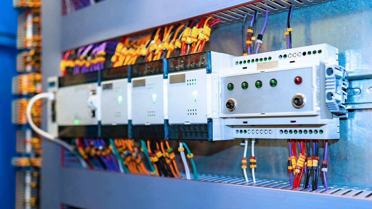
To help meet these requirements, engineers can implement features into their designs such as signal isolation. Signal isolation is an important part of many applications found in explosive environments, such as field transmitters and programmable logic controllers (Figure 1), and is used to improve communication reliability by breaking system ground loops or helping restrict the electrical energy in hazardous environments.

Figure 1: A programmable logic controller in a factory environment

Implementing IECEx-certified digital isolators in explosive environments

While designers have typically turned to optocouplers, also known as optoisolators, for data isolation in explosive environments, digital isolators have emerged as a more performance-optimized approach now that devices are available that were designed to meet the stringent requirements of the IEC 60079. While in the past, most digital isolators could not meet the stringent certification requirements for IECEx and ATEX certifications, that’s no longer the case.

Now that both optocouplers and digital isolators can achieve IECEx and ATEX certification, how do they compare? To provide a comparison, I will use our ISO7041 and ISO7021 digital isolators for reference. Both devices can help designers reduce the explosive potential of their systems. Learn more about key requirements of these standards when designing for explosive environments in the application report, “Intrinsic Safety Compliance of Digital Isolators in Explosive Atmospheres.”

Comparing IECEx-certified digital isolators and optocouplers

At 10 kbps, all four channels of the ISO7041 consume less than 20 µA, enabling you to redistribute the power saved (compared to an optocoupler solution) to other systems in order to improve functionality or add features. Optocouplers typically consume a minimum of 6 mA (10 mA typical) at the device input and several additional milliamps on its output. It is possible to source lower-power optocouplers that consume about 1 mA to 2 mA per channel, but these devices will increase costs. A two or four-channel digital isolator can operate at up to 4 Mbps per channel while consuming very low power for simple two-way communication. This opens up new data-transfer possibilities and capabilities compared to a typical optocoupler, which can only operate at around 100 kbps. Higher-speed optocouplers are available, but they come with the trade-offs of higher power consumption and cost.

Digital isolators also provide a more compact design and a lower package height. The ISO7041 offers four channels of data isolation across 17.5 mm2 of area with a height requirement of 2.5 mm, whereas an optocoupler could consume as much as 50 mm2 depending on the number of data lines.

Digital isolators like the ISO7041 and ISO7021 that use TI’s capacitive isolation technology, where the high-voltage silicon dioxide capacitors provide a high level of isolation and are constructed in a well-controlled semiconductor process, offer very low device variation. In contrast, optocouplers can have significant manufacturing variability and no TDDB (time-dependent dielectric breakdown) requirement, which is a rigorous and standardized dielectric lifetime assessment.

You can learn more about the device reliability and size advantages of digital isolators in field transmitter designs when compared to optocouplers in the application note, “How to Isolate Two-Wire Loop-Powered Field Transmitters.”

If you’ve been designing with optocouplers and are ready to consider a digital isolator, table 1 provides the safety or entity parameters and temperature ratings by application scenario for the ISO7041 and ISO7021, based on the ambient temperature range and maximum input power available on each side of the isolation barrier.

Device

Application

Entity parameters side 1

Entity parameters side 2

Ambient temperature

Maximum component temperature

ISO7041

IS to IS*: case 1

Ui = 50 V

li = 300 mA

Pi = 1.3 W

Li = 0 H

Ci = 4 pF

Ui = 50 V

li = 300 mA

Pi = 1.3 W

Li = 0 H

Ci = 4 pF

-55°C to +70°C

194.3°C

ISO7041

IS to IS: case 2

Ui = 50 V

li = 300 mA

Pi = 1.1 W

Li = 0 H

Ci = 4 pF

Ui = 50 V

li = 300 mA

Pi = 1.1 W

Li = 0 H

Ci = 4 pF

-55°C to +85°C

183.1°C

ISO7021

IS to IS: case 1

Ui = 50 V

li = 300 mA

Pi = 1.3 W

Li = 0 H

Ci = 4 pF

Ui = 50 V

li = 300 mA

Pi = 1.3 W

Li = 0 H

Ci = 4 pF

-55°C to +85°C

183°C

* Intrinsically safe to intrinsically safe (IS to IS)

Table 1: Entity parameters and temperature ratings for digital isolators

Since the maximum component temperature of the ISO7041 and ISO7021 in each scenario above is <200°C, these digital isolators are a good fit for equipment rated to temperature classes T3, T2, or T1 within the specified ambient temperature ranges.

Because certified digital isolators enable you to reallocate the power budget for the rest of the system while providing longer lifetimes and increased reliability, they’re an exciting option for complicated and design-limited applications in explosive environments. If you design systems like these and are considering using a digital isolator approach for the first time but have questions, we can help. Post your need or question in our Isolation forum, and one of our engineers will be in touch.

Adding USB Type-C® with USB Power Delivery to battery-powered applications

$
0
0

Upal Patel co-authored this article.

A USB Type-C® port with USB Power Delivery (PD) is becoming the standard port for charging single- and multicell battery-powered devices. Applications such as wireless speakers, power banks and power tools have been transitioning from proprietary charging ports, legacy USB ports and barrel-jack ports to a standardized USB PD port. USB PD offers a universal alternative for fast and convenient charging, removing the need for users to carry around several adapters or cables with them – helping design engineers create smaller applications with faster charging and fewer components.

As these applications become more feature-rich, compact and power-hungry, it becomes necessary to deliver more power in a smaller solution size. Concurrently, consumers are beginning to expect USB Type-C on their new devices. But implementing a USB PD port has historically been quite challenging for product developers.

Simplifying your design challenge

In the past, adding a USB PD port required a very in-depth understanding of USB specifications and a large firmware and hardware development effort. Several different components need to work together in order to facilitate USB PD support. The two main integrated circuits (ICs) required to complete a USB PD port for charging applications are the USB PD controller IC and battery-charger IC. These ICs typically operate independently of one another and cannot work in a system without a lot of involvement from an external microcontroller (MCU).

This limitation also then requires MCU firmware development in order to communicate events happening on the USB PD port to the battery-charger IC. For example, once the USB PD controller IC negotiates a new voltage and current on the USB Type-C port (or a new power contract), the microcontroller needs to read this information back from the USB PD controller and then update the battery chargers’ charge current and charge voltage based on what’s connected to the USB PD port. Additionally, sourcing power out of the USB PD port to charge external devices requires additional communication between the USB PD controller, MCU and battery charger.

Programming the MCU to interface between the USB PD controller and battery charger is usually not the only firmware development required when adding USB PD. Typical PD controller ICs require some form of firmware development to configure the PD controller behavior itself, such as compiling some code or scripting functions together. Configuring the USB PD controller is necessary in order to ensure that the settings on the PD controller meet your system requirements, including which voltages and currents the system can sink and which ones it can source.

Designing with TI controllers and chargers

To help simplify the design of a USB PD port for battery-powered applications up to 45 W, the TPS25750 USB PD controller adds I2C host support to directly control the BQ25792 battery charger without any intervention from an external MCU. The TPS25750 USB PD controller will automatically update the charging parameters of the BQ25792 over I2C based on the power negotiation over the USB PD port. Thus, the external MCU is now unnecessary, and you don’t need to develop firmware to add a USB PD port to battery-powered applications.

Configuring USB PD port behavior with the TPS25750’s web-based graphical user interface (GUI) entails answering a few multiple-choice questions about what your USB PD port needs to support – no complex scripting, code compiling or firmware development is required. This doesn’t just reduce bill-of-materials costs; it allows you to add USB PD without possessing in-depth expertise about the technology.

The TPS25750 and BQ25792 integrate all of the power paths required for the battery charger and USB PD controller. Figure 1 highlights how these devices simplify the implementation of a USB PD port for battery-powered systems up to 45 W. When using these two ICs together, the USB PD port will be able to support bidirectional power to both source and sink power, thus enabling the system to charge or be charged from the USB PD port when attached to an external device like a laptop, smartphone, headphones or AC adapter.

In addition to these system implementation benefits, the TPS25750D and BQ25792 integrate all of the system’s field-effect transistors (FETs) and remove the need for an external MCU, enabling you to achieve a very small solution size. When compared to an MCU-based nonintegrated USB PD battery-charging implementation, the typical system solution size is around 150 mm2. When using the TPS2570 and BQ25792, it is possible to achieve a system solution size around 55 mm2.


Figure 1: TPS25750D and BQ25792 USB PD battery-charger implementation

Figure 2 highlights an MCU-based USB PD controller and a battery charger with external FETs for applications requiring high-power charging and system power typically greater than 45 W. For applications greater than 45 W, consider pairing the TPS25750 controller with the BQ25731 charger.


Figure 2: MCU-based nonintegrated solution

Table 1 compares USB PD charging for integrated and nonintegrated MCU-based solutions.

USB PD battery-charger implementation up to 45 WMCU-based nonintegrated USB PD battery-charger implementation
External MCUNot required; the TPS25750 is the I2C host controller for the battery chargerRequired; the USB PD controller and battery charger operate independently
Firmware developmentNot required; the system is configurable through a Q&A GUIRequired; necessary to interface with the USB PD controller and battery charger through the MCU
System power pathsAll system power paths are integrated in the USB PD controller and battery chargerExternal FETs are necessary to complete the solution
Solution sizeApproximately 55 mm2Approximately 150 mm2

Table 1: Integrated vs. nonintegrated USB PD battery-charger implementation comparison

The trend toward using USB PD for charging has recently become more urgent, with regulations pushing for universal chargers. Updating your system to charge from USB PD is now easier than ever with the TPS25750 and BQ25792, enabling you to move to the latest universal charging connector while not compromising on solution size.

Interface to sensors in seconds with ASC Studio

$
0
0

You probably find it challenging to set up the various components for your designs. Software development can often be daunting in its complexity, and the added effort of figuring out every component in a system can be intimidating when beginning a design. In order to speed time to market and simplify the software development process when interfacing embedded processing components with analog devices, TI developed an approach that uses intuitive graphical configuration tools to quickly and efficiently generate C code called SysConfig.

SysConfig started as a tool to simplify SimpleLink™ microcontroller (MCU) configurations as shown in Figure 1. The tool brings code examples and full Code Composer Studio™ integrated development environment (IDE) projects to life through a graphical user interface (GUI) that displays all possible configurable parameters. Drop-down menus help you quickly optimize the examples to generate code for the MCU, while tools guide you toward a valid configuration and eliminate the need to search through numerous documents and lines of source code trying to figure out how to update a parameter.

Figure 1: Example LaunchPad™ development kit board view in SysConfig

Our new Analog Signal Chain Studio (ASC Studio) leverages SysConfig , which can be utilized alone or as an extension of this technology, to go beyond pre-configured boards and support a broader TI analog portfolio. Starting with temperature and humidity sensors, ASC Studio makes it easy to quickly set up an interface to supported TI sensors. The graphical setup and configuration of both analog and digital components in a single development environment accelerates the initial setup and configuration of sensors and controllers and gives you more time to create differentiated applications. By combining components in this tool, the GUI automatically avoids conflicts as it generates code.

ASC Studio’s cloud-based interface generates MCU-agnostic code that is 100% portable, commented and C99-compliant (Note: this link requires an active TI.com login in order to enable continuous access to projects over time). For example, let’s say that you selected the TMP117 ultra-high accuracy temperature sensor. After clicking the Add button and selecting configuration settings from the GUI, you can download the .c and .h files for inclusion in an existing project. Figure 2 shows the view of ASC Studio with configurations for a chosen temperature sensor and software files available. This tool enables integration of TI sensors with any development environment and any MCU.

Figure 2: Cloud-based configuration of the TMP117 temperature sensor

If you are also using a SimpleLink MCU in the Code Composer Studio IDE, ASC Studio and the desktop version of SysConfig enable you to generate projects with code already set up for both the sensor and SimpleLink MCU, and begin analyzing data from the sensors in seconds. Here’s how to begin:

1) Install ASC Studio (can be acquired using Resource Explorer in the IDE).

2) Create an empty ASC Studio project:

  • Import an empty software development kit project.
  • Add hardware to the project (such as a BoosterPack™ plug-in module).
  • Add ASC Studio to the project – Figure 3 showcases this view in Code Composer Studio.

Figure 3: Adding ASC Studio to a project

3) Add a sensor to the project:

  • Add a sensor and configure it.
  • Resolve any warnings or errors.

4) Read data from the sensor:

  • Update empty.c to read sensor data.
  • Build and debug.
  • Visualize sensor data.

Along with generating code and creating a sample project, ASC Studio and SysConfig desktop tools also enable quick debugging. The SimpleLink Academy training explains how you can use debugger breakpoints and raw memory displays to check the code, as well as create visualizations to see sensor data running in real time and ensure that the results match your expectations.

TI will continue to add new and existing temperature and humidity sensors to ASC Studio, with plans to include current/voltage/power monitors in the future, enabling you to spend more time on your application and less time with initial setup, interfacing and configuration.

Additional resources

Connecting the dots: How automotive gateways can advance and enhance the driving experience

$
0
0

Automotive suppliers and original equipment manufacturers are heavily investing software R&D efforts on adding new functions and features to achieve autonomy, electrification and connectivity. Still, enabling these functions by adding more electronic control units (ECUs) is not sustainable when it results in increased complexity and cost. 

There are two ways to consolidate and streamline ECUs within a vehicle: using a domain architecture or a zone architecture. A domain architecture consolidates a subset of the ECUs supporting a particular function of the car whereas a zone architecture consolidates ECUs based on their location in the car (ex: the right front zone). Though you could use both approaches to minimize system complexity and cost, a zone architecture streamlines processing and can help further minimize wiring within a car.

Figure 1 illustrates a zone vehicle architecture.


Figure 1: A zone architecture with the DRA821U as a central gateway or a zone gateway in the car

To support the zone architecture, there will be zone gateways that maintain existing Controller Area Network (CAN) and Local Interconnect Network (LIN) communication between ECUs within a specific location while also connecting to a central gateway and other zone gateways using high-bandwidth Gigabit Ethernet. 

The automotive industry has expressed how critical it is for gateway systems to support and bridge multiple interfaces. The DRA821 processor brings gateways with flexible vehicle networking to manage the exploding amount of data in vehicles. It has a rich and diverse set of networking interfaces including legacy CAN and LIN, high-speed PCI Express, and a time-sensitive networking (TSN)-enabled Ethernet switch to support zone architectures. 

When leveraging the zone architecture for additional capabilities, you may encounter limitations when consolidating non-safety-critical and safety-critical ECUs. It’s important to keep mixed criticality (the ability to support safety-critical and non-safety-critical operations within one chip) in mind when suppliers move to minimize complexity while adding capabilities. In the case of gateways, mixed criticality helps maintain an effective network between zones, such as advanced driver assistance system compute module communicating with the braking system, while adding features like cloud connectivity. 

TI has enabled mixed criticality by using extensive firewalls on DRA821 processors to achieve freedom from interference. The device has a total of four Arm® Cortex®-R5F microcontroller (MCU) cores that can support time-sensitive tasks and run in lockstep to support safety. Firewalling these MCU cores as well as the CAN/LIN interfaces, on-chip memory and double-data-rate interfaces from the rest of the chip can support safety-critical functions. Instead of using a separate application processor, you can leverage the dual Cortex-A72 cores isolated from the safety-critical functions for features such as managing the connection to the cloud to create novel business models and user experiences, including over-the-air updates and predictive maintenance. This separation of critical and non-critical functions using the freedom from interference enabled by the DRA821 encourages the integration of innovative features into the gateway while minimizing vehicle network complexity.

While performance requirements and features evolve, the goal of minimizing overall cost remains constant. Gateways require external Ethernet switches to support new vehicle architectures in addition to the safety MCU required for functional safety. The DRA821 can integrate the safety MCU and external Ethernet switch to achieve system cost savings while also enabling zone-based vehicle architectures, as shown in the “Automotive and IoT Gateway Reference Design Based on the Jacinto DRA821 Processor” reference design.

With years of experience in the automotive industry, we know that scaling our customers’ software efforts across different performance points is important. Instead of starting from scratch with another processor, the ability to reuse software allows automotive suppliers to minimize software R&D and reduce time to market. The DRA821 aims to enable advanced networking for vehicles across a broad range of central, domain or zone gateways.

The road to safer, cleaner and more connected vehicles brings many challenges. Suppliers must manage growing system requirements as they continue to innovate while being cognizant of system cost and complexity. With a scalable performance offering and an evaluation module to start software development, the DRA821 is a system-on-chip that brings efficient networking and mixed criticality to feature-rich vehicle gateway systems.

How GaN FETs with integrated drivers and self-protection will enable the next generation of industrial power designs

$
0
0

Physics has caught up with silicon devices. The traditional workhorses of power supplies – metal-oxide semiconductor field-effect transistors (MOSFETs) and insulated gate bipolar transistors (IGBTs) – can only boost power density if you sacrifice efficiency, form factor and heat dissipation.

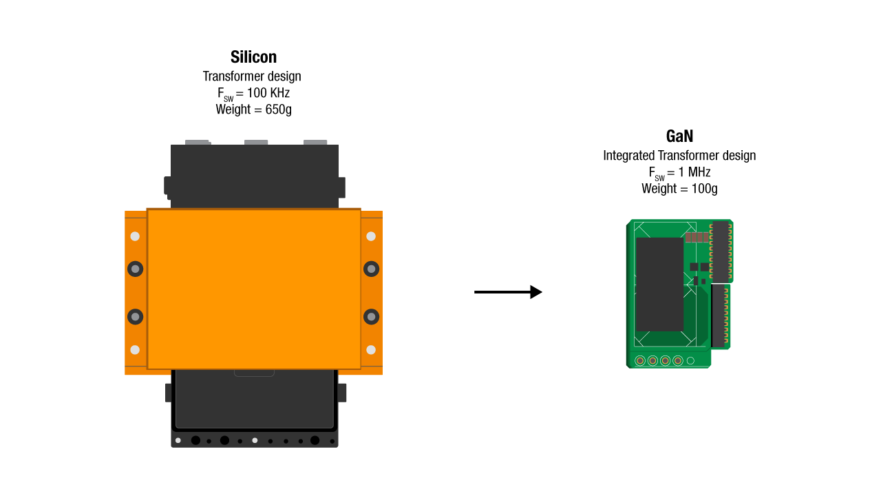
Enter gallium nitride (GaN) semiconductors, which can process power electronics faster and deliver power more efficiently for a growing number of high-voltage applications. GaN’s higher switching capabilities mean that it can convert higher levels of power more efficiently, with fewer components, as shown below in Figure 1. GaN semiconductors enable a new breed of power-supply and conversion systems in AC/DC power delivery applications, such as 5G telecom rectifiers and server computing. GaN is pushing the limits in new applications, and beginning to replace traditional silicon-based power solutions in automotive, industrial and renewable energy markets.

Figure 1: Comparing the power density of the magnetics of silicon designs vs. GaN designs

GaN FETs: new integration venues

Large-scale data centers, enterprise servers and telecom switching centers consume large amounts of power. In these power systems, FETs are typically packaged separately from their gate drivers because they use different process technologies, and end up creating additional parasitic inductance.

That, besides a larger form factor, can limit GaN switching performance at high slew rates. On the other hand, a TI GaN FET with an integrated gate driver, such as the LMG3425R030, can minimize parasitic inductance with a slew rate of 150 V/ns, while providing 66% lower losses and greater mitigation of electromagnetic interference compared to discrete GaN FETs. Figure 2 illustrates a TI GaN FET with an integrated gate driver.

Figure 2: The integration of a 600-V GaN FET with a gate driver and short-circuit protection

In data centers and server farms, TI’s new GaN FETs enable simpler topologies, such as totem-pole power factor correction, which in turn lower conversion losses, simplify thermal design and lead to smaller heat sinks. These devices enable twice as much power density compared to silicon MOSFETs in the same-size 1U rack server while achieving 99% efficiency. This power-density and efficiency savings become especially important when considering long-term impacts. For example, let’s say that a server farm is increasing their AC/DC efficiency 3% each month by installing GaN devices. If that server farm that converts 30 kW of power daily, they would save more than 27 kW a month, which is roughly $2,000 monthly and $24,000 annually.

When a GaN FET is integrated with current-limiting and overtemperature detection, it can protect against shoot-through and thermal runaway events. Additionally, system interface signals enable self-monitoring capability.

Reliability is a crucial factor in power electronics. Therefore, compared with traditional cascade and stand-alone GaN FETs, a highly integrated GaN device can more effectively boost reliability and optimize the performance of high-voltage power supplies by integrating functional and protection features.

With an external driver, parasitic inductance can cause switching losses as well as ringing and reliability issues at high GaN frequencies. Common source inductance increases turnon losses significantly. Likewise, designing a robust overcurrent protection circuit at a high slew rate is difficult and costly. But GaN naturally lacks a body diode, which leads to less ringing on switch nodes and eliminates any reverse-recovery losses.

GaN devices with protection features

GaN devices have very different constructions than silicon devices. Although they can switch faster and harder, there are unique challenges from performance and reliability standpoints. There are also issues such as design simplicity and bill-of-materials cost when using discrete GaN devices.

A new family of industrial, 600-V GaN devices integrates a GaN FET, driver and protection features at 30- and 50-mΩ power stages to provide a single-chip solution for applications ranging from sub-100 W to 10 kW. LMG3422R030, LMG3425R030, LMG3422R050 and LMG3425R050 GaN devices are targeted at high-power-density and high-efficiency applications.

Unlike silicon MOSFETs, GaN conducts in the third quadrant in a “diode-like” manner and minimizes dead time by reducing the voltage drop. TI’s ideal diode mode in the LMG3425R030 and LMG3425R050 further minimizes losses in power delivery applications. Read the application note, “Maximizing the Performance of GaN with Ideal Diode Mode,” to learn more.

These GaN devices have gone through 40 million hours of device reliability testing, including accelerated and in-application hard-switch testing. The reliability tests occurred under highly accelerated switching conditions at maximum power, voltage and temperature environments.

Conclusion

Designers of switching power supplies are continually trying to raise power density while increasing efficiency. While silicon MOSFETs and IGBTs offer low power density and efficiency, silicon carbide (SiC) devices facilitate higher power density and efficiency at a greater cost.

GaN devices enable solutions with twice the power density of what is possible with best-in-class superjunction FETs. Likewise, they facilitate qualification to standards like 80 Plus Titanium that demand very high efficiency for power supplies in server and telecom applications.

While GaN is a game-changing technology for power electronics, it also demands thorough process and materials engineering. That calls for growing high-quality GaN crystal, optimizing the dielectric films and achieving very clean interfaces in the fabrication process. Masterful testing and packaging are also a must.

2 ways to zero out signal-chain errors with chopper amplifiers

$
0
0

As the need for higher resolution and higher-speed signal chains increases for industrial equipment such as programmable logic controllers, weigh scales and automated test equipment, so does the need for high-precision amplifiers acting as analog-to-digital converter (ADC) drivers and voltage reference buffers in such signal chains.

In this article, I’ll discuss two common design challenges when designing a precision signal chain, and how to overcome them. But first, it’s important to understand chopper amplifiers, which are popular in these systems.

What is a chopper amplifier?

A chopper amplifier is a type of zero-drift operational amplifier (op amp) known for having a very low offset voltage, thanks to an internal topology that minimizes the amplifier’s offset regardless of configuration. This results in very low offset errors (offset, drift, common-mode rejection ratio [CMRR], power-supply rejection ratio [PSRR] and open-loop voltage gain [Aol]), as shown in Figure 1. Another benefit of this topology is that it has flat 1/f or flicker noise, since the amplifier perceives (and thus minimizes) low-frequency noise as a DC error. Chopper amplifiers are an excellent choice for applications requiring high precision across frequencies ranging from DC to tens of kilohertz, such as precision temperature monitoring, Wheatstone bridge measurements and voltage reference buffering.

Graph and spec differences show that chopper amplifiers have low offset errors and flat 1/f noise curve due to architecture as compared to continuous-time amplifier.

Figure 1: Chopper amplifiers have low offset errors and a flat 1/f noise curve due to their architecture

Now, let’s get back to the challenges facing precision signal chains.

Challenge No. 1: minimizing offset errors across temperature

One of the biggest challenges when designing a precision signal chain is minimizing the offset errors introduced by the ADC driver and reference buffer. While performing calibration during production can improve offset, CMRR, PSRR and Aol performance, offset voltage drift is difficult and expensive to calibrate It requires changing the system temperature in production or adding a calibration loop, which increases system size and bill-of-materials count. Instead of calibrating for offset drift, using a chopper amplifier helps resolve this issue thanks to its inherently low offset drift performance.

However, there’s a new problem with the next generation of chopper amplifiers that limits these devices from achieving even better offset drift. This problem is known as the Seebeck effect, which is a part of the thermocouple effect. The Seebeck effect is the generation of an electric potential across a temperature gradient, which naturally occurs in an amplifier that self-heats during operation, as well as the ambient temperature. This gradient increases in a device that uses dissimilar metals in the signal path, from the pins to the amplifier core.

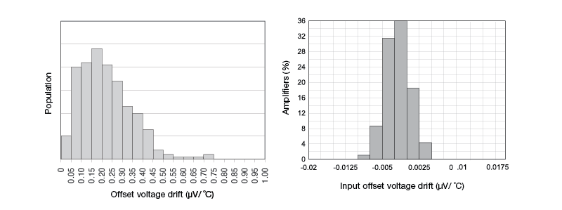
Upon recognizing this limitation and performing extensive experiments with different materials, TI identified a material combination that enabled the production of the OPA2182 with a maximum of only 12 nV/°C of offset drift across the full temperature range of -40°C to +125°C. Figure 2 compares the offset drift of the OPA2182 with a nonchopper amplifier, the OPA2140.

Two graphs show the difference in input offset drift between OPA2182 and OPA2140.

Figure 2: OPA2182 offset drift vs. OPA2140 laser-trimmed offset drift


Challenge No. 2: improving signal settling time

Another challenge when designing a precision signal chain is how to quickly and accurately settle the signal at the input of the ADC. Settling is particularly difficult for systems that use a multiplexer at the input to the signal chain to save both board space and system cost. The issue that arises with a switched input is that when the multiplexer switches channels, the ADC driver may see a step input. Many amplifiers have anti-parallel diodes connected between them for protection. When subjected to a step response, the inputs will no longer be approximately equal (as they are under normal operation), and one of the anti-parallel diodes will become forward-biased, drawing current from one input to the other. This current will flow through the multiplexer and the signal source, causing a delayed settling response.

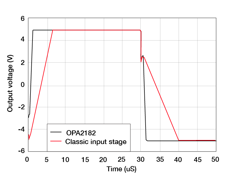
To improve the settling time of the amplifier, TI added multiplexer (MUX)-friendly inputs to devices such as the OPA2182. This patented structure removes the anti-parallel diodes and enables the amplifier to settle a step input faster, as there is no erroneous current flowing through the signal source and multiplexer. Figure 3 compares the settling time of MUX-friendly inputs with a classic input stage.

Graph shows difference in output voltage over time between the MUX-friendly OPA2182 vs. classic input stage

Figure 3: Settling time of the OPA2182: a MUX-friendly input vs. a classic input stage


Although many challenges exist when designing a precision signal chain, chopper amplifiers like the OPA2182 can help simplify your designs, thanks to their improved offset drift performance and MUX-friendly inputs.


Powering levels of autonomy: a quick guide to DC/DC solutions for SAE autonomy levels

$
0
0

Most of today’s automotive vehicles use some level of autonomy. The Society of Automotive Engineers (SAE) defines five levels of autonomy, from level 0 to level 5 (Figure 1). In this technical article, I’ll discuss the DC/DC power-supply needs for each autonomy level. I hope that design engineers looking to understand the power-supply challenges and requirements of automotive applications at various autonomy levels will find this guide helpful.


Figure 1: Levels of driving automation (courtesy of SAE)

Levels 0 and 1

Rear view cameras are an ADAS feature often found in level 0 and 1 autonomy. Mostly powered directly from the car battery and sometimes tied to the rear light assembly, rearview cameras require small DC/DC converters like the LMR34206-Q1 and LMR34215-Q1 with good noise reduction and low ripple. The sensor inside the camera module is highly sensitive to noise from dark currents created by heat, but also to noise injected from or through the power supply. A compact and low-noise low-dropout regulator (LDO) like the LP5907-Q1 can help manage unwanted noise in the system.

Forward-facing camera systems, also present in level 1, use machine vision to identify objects and perceive the road situation ahead of the car as the vehicle travels at higher speeds, requiring higher data-processing speeds than rearview cameras and lower levels of latency. As such, these systems need more software and more power for data processing, requiring high-efficiency converters like the LM62440-Q1 or LM61440-Q1 to help reduce thermals and lower electromagnetic conduction.

Level 2

Level 2 involves partial automation and includes the control of two vehicle movements at the same time, e.g. steering and accelerating. Most high-end (and some mid-range) vehicles are at this level. As the number of sensors grows, so do the power needs.

Figure 1 shows a typical block diagram of a radar power management system, which comprises a small electronic control unit (ECU) that needs a power supply with a low bill of materials, such as the LM63625-Q1, and a second-stage power-management integrated circuit (PMIC) such as the LP87702-Q1. These device families are scalable across various power levels for different radar types (such as corner, front and side), and since they have the same pinout and footprint, you can use them across a variety of designs.


Figure 2: Typical power block diagram of a radar system

Level 3

Level 3 involves conditional automation. The driver can now let go of the steering wheel, accelerator and brakes, but some road conditions will need the driver to resume control. Level 3 increases the processing needs of the ECUs used in autonomous systems, as vehicles now have to integrate information from various sensors to make decisions (a process called sensor fusion). As the power increases, a potential power component choice for a forward-facing camera or cascaded radar could be the LM61460-Q1 buck converter, as it can support the increased need for processing power.

Automakers use varying quantities and types of sensors to implement different levels of autonomy; this often means that the processors need scalability in order to meet additional performance needs, and flexibility as power requirements change. In such instances, you might not be able to support these power needs with a single PMIC, and will require smaller and more flexible products. The TPS628501-Q1 and TPS628502-Q1 come in a small-outline transistor (SOT)-583 package, but have tight output tolerance and control loops to support fast-acting transients for data processing and low latency.

Levels 4 and 5

Level 4 is called high automation; the car now works with features of full autonomy. Although the driver can take control of the vehicle, the car is capable of performing various maneuvers without driver intervention. The final level of autonomy, level 5, is defined as full autonomy, where the vehicle has full control and no conditions exist where the driver (now essentially a passenger) can operate the vehicle. Levels 4 and 5 both require the highest level of sensor data and incorporate lidar, which offers a 3D map of the environment and provides high quantities of data. Should lidar or radar fail for any reason, the vehicle will go into “limp home” mode and use other sensors as backup.

For such high-power applications, consider the LM61495-Q1. This is one device in a highly integrated converter family which is pin compatible and supports 6 A to 10 A to supply the system requirements. For even higher levels of power, a device like the LM5143-Q1 can support in excess of 20 A, and multiple phases, helping support the power needs as well as cancelling noise and reducing component count.

Conclusion

As the level of autonomy increases so does the power needs of the system, this will potentially mean new types of power devices and architectures. Close consideration should be paid also to the system sensitivity to noise, size and cost.

Additional resources

How Wi-SUN FAN improves connected infrastructures

$
0
0

Most modern Internet-of-Things appliances and devices can be monitored, controlled and activated from anywhere in the world. These things generate data regularly, and collectively they account for a massive amount of data. To access information and services quickly and reliably, companies across all sectors are more invested in connectivity, which entails faster, more reliable networks and better encryption and security.

Smart cities have the potential to better people’s lives by bridging the gap between the connected consumer and a connected infrastructure. Imagine a world where you save time getting to your flight because an application in your cellphone let you know of an open parking spot on level 4, or if traffic lights could more dynamically control traffic flow to ease commutes. Imagine if a connected lighting pole in front of your house could communicate with the utility company when the lights go out.

Connectivity is a key part of making this a reality.

Utilities and companies developing products for smart cities have several connectivity options, and the Wi-SUN field area network (FAN) is a good option. Why? Let’s start by considering its reliability.

Most common network topologies are star or mesh; Wi-SUN is a mesh network (shown in Figure 1).


Figure 1: Example of mesh network

The star topology is simple and easy to configure, having a hierarchical structure, where bridges and switches are normally connected to a small number of end nodes. Because of its structure, it can have a single point of failure, which may cause concerns when a field crew must perform maintenance or replace a malfunctioning device to keep the network up and running.

A mesh topology is not a hierarchical structure, and as such, you can add routers dynamically to the network to extend the range of a node, using self-configuration to connect to other routers. In the event of a router failure, the network will go into “self-healing” mode, during which the routers find another available connection to allow traffic to continue. What does that mean for end users? A more robust network and reduced downtime for the thousands of connected nodes.

Wi-SUN is based on a frequency-hopping scheme, which contributes to its robustness and reliability because it reduces potential packet losses caused by interference from other networks, especially in high-density areas like city downtowns. Frequency hopping also makes it possible to transmit high-output power in Canada and in the Americas, up to +30 dBm.

Wi-SUN supports a range of data rates, trading off coverage versus throughput. This enables the Wi-SUN FAN to meet the needs of a wide range of network deployment applications, like electric vehicle charging stations, smart transportation, smart parking, environmental sensors and traffic management (Figure 2). Consider the smart city example – throughput and coverage needs can vary widely among certain applications. Smart meters and smart parking, for example, have a need to transmit different amounts of data. The Wi-SUN FAN can scale as needed to meet these varied demands, enabling the applications illustrated below.

Figure 2: Example of potential applications using the Wi-SUN FAN

Another concern that Wi-SUN addresses is security. Hackers are sharpening their skills by the minute, and networks must be resilient against potential threats designed to steal data. Wi-SUN has a security profile that uses device certificates authenticated by trusted root certification authorities to prevent unauthorized network access. It also uses cryptoalgorithms such as elliptic curve Diffie-Hellman, elliptic curve digital signature algorithm and Advanced Encryption Standard-128 cipher block chaining-message authentication code to preserve message confidentiality and integrity. This is important when adding new devices to the network and enabling their identification and authentication. Wi-SUN equipment manufacturers can even obtain a cybersecurity certificate indicating compliance with the FAN Technical Profile Specification.

Because Wi-SUN provides scalability reliability, security and high speed, you may be wondering if it is costly. The good news is that Wi-SUN is an open-standard solution, based on the Institute of Electrical and Electronics Engineers (IEEE) 802.15.4g wireless standard. As an open standard, it allows the interoperability of equipment from different manufacturers, which may translate to competitive prices for consumers. To guarantee compatibility, manufacturers must go through a formal certification process, which should give city managers and utility companies peace of mind.

As of this month, there are more than 230 members of the Wi-SUN alliance representing 26 countries, with more than 96 million devices deployed worldwide.

Texas Instruments provides transceivers and network processors that support Wi-SUN FAN 1.0. For example, the low-power and high-performance CC1200 wireless transceiver supports a maximum transmission data rate of 1 Mbps and has a sensitivity of -122 dBm at 1.2 kbps, which translates to high speed and long range. It also meets North American, European and Japanese standards.

For developers looking for a network processor, CC1312R and CC1352P wireless microcontrollers include a 48-MHz Arm® Cortex® M4F, with flash memory (so you can update your firmware over the air) and a cryptoaccelerator for security purposes.

Wi-SUN brings these benefits to utilities, equipment manufacturers and end users:

  • A robust network with low downtime due its mesh configuration.
  • A reliable communication technology that uses frequency-hopping scheme, resulting in a very low number of packet losses in noisy and high-density areas.
  • A secure network through a well-defined security profile.

Additional resources

Designing TI mmWave radar made easier using our third-party ecosystem

$
0
0
If you are new to radar or interested in replacing your existing sensing technology with radar, there can be a significant learning curve to both designing your product and ramping to production. In order to lower this barrier, Texas Instruments created...(read more)

Powering medical imaging applications with DC/DC buck converters

$
0
0

From cart-based ultrasound scanners to portable smart probes that send images directly to a smartphone, the world of ultrasound imaging continues to diversify. Despite architectural differences in their design, every ultrasound system needs a DC power supply that can efficiently meet the power demands of the system and avoid interference with the ultrasound frequency range. In this article, I will review the primary design challenges when selecting a DC/DC buck regulator for medical ultrasound systems.

Synchronizing to external clock and minimizing interference

The buck regulator in the power supply must be able to synchronize to an external clock frequency. The ultrasound frequency band used for medical imaging is typically within the range of 2 MHz to 20 MHz. Therefore, when designing a switch-mode power supply for any ultrasound system, it is imperative that the switching frequency of the buck regulator does not interfere with the ultrasound band. A buck regulator with a low switching frequency will keep the fundamental and early harmonic frequencies out of the ultrasound band, but some harmonics will still persist. By synchronizing the switching frequency of the buck regulator to an external master clock, you can control, monitor and precisely filter the switching frequency and its harmonics out of the ultrasound band.

While I’m on the topic of interference, it is also important to keep in mind the intrinsic electromagnetic interference (EMI) produced by any buck regulator in an ultrasound power supply. Even when the switching frequency and its harmonics are filtered, buck regulator can generate broadband frequencies that interfere with the rest of the system. Proper printed circuit board layout can greatly improve EMI, but to achieve optimum performance, consider using a buck regulator specifically designed to have low EMI. The LMQ61460, for example, has integrated bypass capacitors in addition to other design features (like external frequency synchronization) that minimize EMI. To confirm that a device truly has low EMI, check to see if the data sheet includes data from radiated or conducted EMI testing (or both) in the Other Common Conditions section. Figure 1 shows the conducted EMI of the LMQ61460.


Figure 1: Conducted EMI of the LMQ61460 versus Comité International Spécial des Perturbations Radio 25 (limits: yellow, peak signal; blue: average signal; FSW = 400 kHz; VOUT = 5 V; IOUT = 5 A)

Scaling to multiple power rails

A buck regulator that can handle multiple current and voltage requirements, including negative voltage rails, can be highly advantageous. Ultrasound systems typically have multiple power rails, each designed to rest at a different voltage and deliver a different current. You can use a device with a wide input voltage range, wide output voltage range and high-enough current limit to scale one power solution to all needed power rails (including negative output rails).

Leveraging one device to power all of the rails can help you optimize the system’s bill of materials (BOM) and simplify the layout process; if these benefits are important to you, consider a module approach. Figure 2 shows a portion of the block diagram for Programmable Ultrasound Power Supply Reference Design. The LMZ34202 is a buck converter module with an integrated output inductor that is used in the mentioned reference design to regulate the positive voltage rails, with a separate module, LMZ34002, used for the negative voltage rail, VEE. This is a perfectly acceptable design. But if the designer wanted to further simplify BOM and layout process, he or she could have used a device with a higher current rating, say the TPSM53604. The higher 4-A current rating of this buck power module would have allowed it to regulate the 5-V as well as -5-V rail.

Figure 2: Three separate power rails. Two regulated with the LMZ34202 and one regulated with the LMZ34002.

Ensuring high efficiency and power density

The medical industry continues its push to make ultrasounds more accessible by making them more portable. For battery-powered systems like portable ultrasounds and smart probes, the efficiency of the buck regulator under all operating conditions is essential to maximizing battery life. Portable applications also present the challenge of limited space. Although these are valuable features in stationary ultrasounds, to improve the portability of your system, consider selecting a buck regulator with:

  • High efficiency at the preferred operating switching frequency.
  • Low quiescent current to reduce battery drain during no-load and light-load conditions.
  • High power density to save space.

Of course, it can be difficult to achieve high efficiency and high power density when working with switching power supplies that require additional filtering to minimize noise. In such scenarios, you might choose to work with specialized DC/DC buck converters, such as the low-noise and low-ripple TPS62912 or TPS62913, which offer excellent efficiency as well as external clock synchronization, and use integrated ferrite-bead filter compensation to filter out high-frequency noise.

Conclusion

When designing a DC/DC power supply for ultrasound, consider the unique demands of the system. The ability to synchronize to an external clock is paramount in order to effectively reduce and control harmonics in the ultrasound band. A buck regulator with a wide input voltage, wide output voltage and acceptable current limit will enable you to scale your solution and optimize your BOM. Finally, when selecting buck converters for portable applications, consider features such as high power density, high efficiency and low quiescent current to maximize efficiency.

Additional resources

Lighting the way with DLP automotive headlights

$
0
0

Recently, there has been a big push in the automotive lighting industry to improve both vehicle headlight functionality and driver visibility, which has led to the development of adaptive driving beam (ADB) headlights. ADB is an automotive exterior lighting system that automatically controls the high beam, to allow the driver to focus on the road ahead without manually controlling the high beam. DLP automotive technology can be used to enable ADB systems with over 1.3 million pixels to project more light on the road. In addition to ADB, headlights with DLP automotive headlights can enable many new features.

Download our white paper, improving visibility with DLP® headlights, to learn more about how DLP technology can improve the functionality of your vehicle headlights.

Evolving technologies

Although the DLP5533A-Q1 digital micromirror device (DMD) was designed to improve ADB resolution and help vehicles maximize the amount of light on the road, new applications are constantly being enabled such as, structured light to warn driver of upcoming hazards, traffic sign dimming to improve ADAS performance, and weather detection to help the vehicle adapt to surrounding conditions.

Viewing all 4543 articles
Browse latest View live


<script src="https://jsc.adskeeper.com/r/s/rssing.com.1596347.js" async> </script>