Quantcast
Channel: TI E2E support forums
Viewing all 4543 articles
Browse latest View live

Automotive GaN FETs engineered for high frequency and robustness in HEV/EVs

$
0
0

Intent on accelerating electric vehicle (EV) adoption by addressing top consumer concerns such as driving range, charge time and affordability, automakers worldwide are demanding increased battery capacity and faster charging capability, with little to no increase in size, weight or component cost.

The EV onboard charger (OBC), which allows consumers to recharge the battery directly from an AC main at home or at public or commercial outlets, is undergoing rapid changes. The need to increase charging rates has led to an increase in power levels from 3.6 kW to 22 kW, but at the same time, the OBC must fit inside the existing mechanical envelope and carried around by the car at all times without impacting driving ranges. Finally, there’s a movement to increase OBC power densities from <2 kW/L today to >4 kW/L.

The impact of switching frequency

The OBC is essentially a switch-mode power converter. Passive components such as transformers, inductors, filters and capacitors, along with heat sinks, constitute the bulk of its weight and size. Increasing the switching frequency means smaller passive components. A higher switching frequency, however, causes higher power dissipation in switching elements like power metal-oxide semiconductors (MOSFETs) and insulated gate bipolar transistors.

Reducing size requires a further reduction in power losses to maintain the same component temperatures, as there is a smaller surface area available now to extract heat. This higher power density demands a simultaneous increase in switching frequency as well as efficiency. And therein lies the challenge, which silicon-based power devices struggle to deliver.

Increasing the switching speed (how fast the voltages and currents change between the terminals of the device) will fundamentally reduce the switching energy losses. This is necessary, or else the practical maximum frequency is limited. Power devices with lower parasitic capacitance between their terminals – that are designed carefully in low-inductance circuit-path arrangements – offer a path forward.

Going beyond silicon

Power devices built using wide band-gap semiconductors such as gallium nitride (GaN) and silicon carbide (SiC) offer dramatically lower capacitance for a comparable on-resistance and breakdown voltage by virtue of their device physics. Higher critical electric fields for breakdown (10 times for GaN vs. silicon) and higher electron mobility (>33% for GaN vs. silicon) effectively enable a lower on-resistance and lower capacitance simultaneously. As a result, GaN and SiC FETs are inherently capable of operating at higher switching speeds with lower losses than silicon.

The advantages of GaN are particularly striking:

  • GaN’s low gate capacitance enables faster turnon and turnoff during hard switching, reducing crossover power losses. GaN’s gate charge figure of merit is 1 nC-Ω.
  • GaN’s low output capacitance enables rapid drain-to-source transitions during soft switching, especially with low load (magnetizing) currents. A typical GaN FET, for instance, has an output charge figure of merit of 5 nC-Ω compared to silicon at 25 nC-Ω. This enables designers to use small dead times and low magnetizing currents, which are necessary to increase the frequency and reduce circulating power losses.
  • Unlike silicon and SiC power MOSFETs, a GaN transistor has no body diode inherently present in its structure, and therefore no reverse-recovery losses. This makes new high-efficiency architectures like totem-pole bridgeless power-factor correction practical at multiple kilowatts, previously impossible with silicon devices.

All of these advantages enable designers to achieve high efficiency at much higher switching frequencies with GaN, as illustrated in Figure 1. GaN FETs, rated to 650 V, enable applications up to 10 kW like server AC/DC power supplies, EV high-voltage DC/DC converters and OBCs (with parallel stacking to reach 22 kW). SiC devices, available up to 1.2 kV with high-current-carrying capabilities, are a good fit for EV traction inverters and large three-phase grid converters.

Figure 1: GaN surpasses all technologies in enabling very high-frequency applications

Design challenges with high frequency

The typical 10-ns rise and fall times when switching several hundred volts require careful design to avoid parasitic stray inductance effects. Common-source and gate-loop inductance between the FET and driver play these critical roles:

  • Common source inductance limits drain-to-source transient voltages (dV/dt) and transient currents (dI/dt), slowing down switching speeds, and increasing overlap losses during hard switching and transition times during soft switching.
  • Gate-loop inductance limits gate-current dI/dt, reducing switching speeds and increasing overlap losses during hard switching. Other negative effects include increasing susceptibility to Miller turnon, causing a risk of additional power losses, and introducing a design challenge to minimize gate insulator voltage overstress, which reduces reliability if not mitigated properly.

As a result, engineers may need to resort to ferrite beads and damping resistors, but these reduce switching speeds and go against the goal to increase frequency. While GaN and SiC devices are intrinsically adaptable for high-frequency operation, extracting their full benefit still means overcoming system-level design challenges. A cleverly engineered product that takes into account ease of use, robustness and design flexibility will accelerate technology adoption.

GaN FET with integrated driver, protection, reporting and power management

Fully integrated, 650-V automotive GaN FETs from Texas Instruments aim to deliver the high-efficiency, high-frequency switching benefits of GaN without the associated design and component-selection drawbacks. The integration of a GaN FET and driver in close proximity within a low-inductance quad flat no-lead (QFN) package significantly reduces parasitic gate-loop inductances, eliminating worry about gate overstress and parasitic Miller turnon, while very low common-source inductance enables fast switching, reducing losses.

The LMG3522R030-Q1, combined with the advanced control features in the C2000™ real-time microcontrollers, such as the TMS320F2838x or the TMS320F28004x, enables switching frequencies greater than 1 MHz in power converters – reducing magnetics size by 59% versus existing silicon and SiC solutions.

Demonstrated drain-to-source slew rates of >100 V/ns make it possible to reduce switching losses by 67% over discrete FETs, while its adjustability between 30 V/ns and 150 V/ns enables trade-offs between efficiency and electromagnetic interference, reducing downstream product design risk. Integrated current protections offer robustness, while new feature additions include digital pulse-width modulation temperature reporting for active power management, state-of-health monitoring and ideal diode mode, as offered in the LMG3525R030-Q1, which eliminates the need for adaptive dead-time control. A 12-mm-by-12-mm top-side cooled QFN package also enables enhanced thermal management.

With more than 40 million device reliability hours and a failure-in-time rate for 10-year lifetimes <1, TI GaN devices offer the ruggedness that automakers expect. Manufactured on widely available silicon substrates and using existing process nodes in 100% internal manufacturing facilities, TI GaN delivers definitive supply-chain and cost advantages, unlike other technologies built on SiC or sapphire substrates. Visit TI GaN online for more information about automotive GaN FETs.


4 key questions about motor design challenges

$
0
0

Stepper motors are an integral part of systems that need precise positioning, excellent speed control and repeatability of movement. You’ll find stepper motors in 3D printers, textile machines, medical tools, robotics, printers, stage lighting and ATMs.

A stepper motor has two electrical current windings controlled with an H-bridge, and moves in discrete steps defined by a step angle. If you’re designing with this kind of motor, you’ll encounter some common challenges, some of which are driver-related, while others are system-related. In this article, I’ll answer some of the most frequently asked questions I receive about how to mitigate these issues, some of which are mapped out in Figure 1.

Figure 1: Common challenges when designing with stepper motors

Q: What is tuning? What causes it, and why is it important?

A: Stepper motor systems must drive and decay current continuously in order to regulate the current and hold the position of the motor at each step. This creates current ripple. Designers use a combination of fast, slow and mixed-decay modes to control the current through the motor windings. The process of selecting the optimal decay mode is called “tuning.”

Tuning is important, as improper tuning can cause vibration and unwarranted audible noise, also shown in Figure 1. Good tuning directly enables smooth motion, reduces audible noise and improves positional accuracy.

TI’s patented smart tune technology is a decay scheme that adapts itself to changing operating conditions and motor parameters, leading to smoother motion for the stepper motor. Cycle by cycle, smart tune automatically optimizes the decay mode to maintain current regulation, keeping the motor running smoothly, quietly and up to 11°C cooler than using a fixed-decay mode, as detailed in the application note, "Smart Tuning for Efficient Stepper Driving." Smart tune also minimizes motor noise and vibration by preventing current regulation loss. More information can be found in the white paper, "Stepper motors made easy with smart tune." Figures 2a, 2b and 2c show instances of untuned waveforms, while Figure 2d shows a perfectly tuned waveform using smart tune.

Figure 2: Different drive and decay states: untuned, with too much fast decay (a); untuned, with a minimum drive time that’s too long (b); untuned, with a large back-electromotive force (EMF) during slow decay (c); tuned waveform approximating a sine wave using the smart tune decay scheme (d)

Q: What causes high audible noise? Is it possible to reduce audible noise in a system?

A: The amount of audible noise from a stepper motor depends on the type of motor and the operating condition. The sources of noise coming out of a stepper motor can be magnetic, mechanical or electrical. The amount of ripple directly affects the amount of electrical noise in the system. One way to ensure minimum ripple control (and thus noise) is to use the smart tune ripple control available in stepper motor drivers like the DRV8426 and DRV8424, where the off-time (TOFF) adjusts based on operation to achieve the target ripple, as shown in Figure 3. More details can be found in the app note, "How to Reduce Audible Noise in Stepper Motors."


Figure 3: Smart tune ripple control


Figure 4 shows the comparison of audible noise performance using smart tune ripple control with a competing device employing mixed decay. The figure clearly shows the DRV8424 performing as much as 10% better.


Figure 4: Audible noise performance using smart tune ripple control vs. a competing device

Q: What causes motors to vibrate? Are there ways to reduce this vibration and increase motion smoothness?

A: Creating a current ripple requires keeping the current regulated and holding the motor position at each step by continuously driving and decaying the winding current. In a traditional system, using a high ratio of slow decay and increasing the motor speed introduces a significant back-EMF voltage, causing current regulation losses, motor vibration and overheating. Because stepper drivers use open-loop control, there is no reference for position. Additionally, poor channel-to-channel current matching, bad current-sense accuracy and low microstepping levels may result in choppy motion.

Smart tune technology in our DRV8426, DRV8428, and DRV8424 stepper motor drivers detects the change in current and automatically inserts a higher ratio of fast decay to keep the motor in regulation. Additionally, these devices provide 1/256 microstepping and integrated current sensing with tight ±5% current-sense accuracy, smoothing the motion of the motor to its intended location as explained in the app note, "How to Improve Motion Smoothness and Accuracy of Stepper Motors."

Q: Are there ways to reduce the bill-of-materials (BOM) cost and system size?

A: Stepper motor drivers typically require two current-shunt sense resistors to monitor and regulate current. These shunt resistors are expensive, increase BOM costs and require additional routing. Our DRV8426, DRV8424, DRV8434 stepper motor drivers integrate current sensing and eliminate the need to use external, bulky, expensive shunt resistors while achieving ±5% current accuracy. More information can be found in the application note, "Advantages of Integrated Current Sensing." Figure 5 compares the DRV8424/DRV8426 evaluation module (EVM) drawn to scale with competing devices, where the DRV8424/DRV8426 EVM is 75% and 50% smaller than competing device 1 and 2 respectively.

Figure 5: EVM size comparison

If you have a question about designing with stepper motor drivers that I didn’t answer, I hope you’ll ask it below or in the TI E2E Motor drivers forum. My colleagues and I can help throughout every step of your design process.


Conserve battery power in HEV/EVs with automatic host reverse wakeup

$
0
0

As more vehicles become electrified, the need to achieve the highest levels of functional safety with high-accuracy battery monitoring is paramount. Yet in order to improve battery-monitoring accuracy, the vehicle’s battery management system must work efficiently in real time to monitor the performance of the individual battery cells within.

In typical hybrid electric vehicle (HEV) and electric vehicle (EV) configurations, the battery management unit (BMU) is powered from a 12-V battery. This battery remains on even when the car is parked or turned off, in order to support features like remote key entry, security and battery monitoring. When the car is parked, to ensure proper health of the battery, the microcontroller (MCU) has to periodically wake up to look for faults in high-voltage battery packs. This periodic wakeup draws current and can prematurely discharge the 12-V battery.

Design engineers and automotive manufacturers can now consider a new automatic host reverse wake-up feature that enables the host MCU to be off and rely instead on a supply power-management integrated circuit (PMIC) to remain in low-power mode and conserve 12-V battery power.

Examining a wake-up-at-fault battery design

As illustrated in Figure 1, EV battery packs can stack up to 800 V and beyond to support the demanding loads of the AC motor. These battery packs comprise hundreds of cells stacked together in series. A distributed battery pack system supports high-cell-count packs by connecting multiple high-accuracy battery monitors on separate printed circuit boards called cell sensing units.

The BMU board holds the host MCU, its supply (a PMIC or system-basis chip [SBC]) and a communication interface, which links the MCU and battery-monitoring devices on the cell monitoring unit, which then connects to the actual battery cells. A ring connection is supported to reverse the daisy-chain communication direction in the event of cable failure. The host MCU interfaces with the control unit of the vehicle through a Controller Area Network bus. By effectively monitoring each battery cell, an EV’s MCU can ensure the proper operation of all battery cells.


Figure 1: Simplified battery management system diagram

Improving accuracy with TI’s battery monitors and balancers

TI’s BQ79616-Q1 battery monitor and balancer can continuously monitor the high-voltage battery even in sleep mode. In case of a fault in the battery, the BQ79616-Q1 transfers the fault information through the daisy-chain configuration to the BQ79600-Q1 communication interface. In turn, the BQ79600-Q1 wakes up and commands the PMIC and MCU to wake up. The MCU does not have to periodically wake up on its own, and can instead rely on the BQ79616-Q1 monitor. Thus, the BQ79600-Q1 – along with the BQ79616-Q1 automatic host reverse wake-up feature – allows the MCU to be off and its PMIC to be in lower-power mode, which minimizes current draw on the 12-V battery and conserves battery power.

As illustrated in Figure 2, when the BQ79616-Q1 is in sleep mode, the low-power operation mode, cell overtemperature and undertemperature, cell overvoltage and undervoltage, and thermistor overtemperature and undertemperature fault detections are still active. Because communication is not available in sleep mode, the device provides an option to transmit the fault status through heartbeat (device in no fault state) and fault (device in fault state) tones.

These tones are transmitted in the same direction as a communication command frame. Unlike communication tones, heartbeat and fault tones are transmitted periodically. The heartbeat and fault tone receivers are always on in sleep mode. For the tone signal to return back to the base device (in order to trigger NFAULT), a ring architecture is necessary to support transmitting fault status in sleep mode. Once the BQ79600-Q1 sniffer detects a fault tone, it puts itself into validate mode to check if a true fault exists or not. If a true fault exists, the BQ79600-Q1 triggers the INH pin, a high-voltage output pin that provides voltage to enable the PMIC.


Figure 2: Automatic host reverse wakeup with TI battery monitors and balancers

Conclusion

The BQ79616-Q1 family of battery monitors and balancers supports automatic host reverse wakeup, which enables the host MCU to remain off and its power supply to be in the lowest-power mode while the BQ79600-Q1 monitors for faults coming from stacked battery-monitoring devices. The BQ79600-Q1 wakes up the SBC through the INH pin, which then further wakes up the MCU if the event of an unmasked fault detected by the BQ79600-Q1 or stacked BQ79616-Q1s. This enables the conservation of 12-V battery power and supports functional safety requirements like cell monitoring for overvoltage, undervoltage, overtemperature, undertemperature, thermistor overtemperature and thermistor undertemperature, even when the EV is parked or turned off.

Additional resources

Increasing flexibility in your precision analog designs with a low-cost MSP430™ MCU

$
0
0

When designing a system, the main goal is to meet high performance requirements at a low overall cost. It’s a delicate balance that influences the architecture of the whole system. Many systems, such as field transmitters, thermometers and electricity meters (also called e-meters) include at least one sensor, which may require an analog front end (AFE) as well. However, simply choosing a fixed-function AFE may not unlock the full potential of your design.

Design choices and flexibility trade-offs

Typically, you select a host microcontroller (MCU) or processor first as the foundation for your design, and then select other building blocks such as power, protection, communication and signal-chain components. If the system includes sensors with low-amplitude or differential outputs, you would probably pick a sigma-delta (also called delta-sigma) analog-to-digital converter (ADC) as the AFE. There are several common AFE options from which to choose, including:

  • Discrete sigma-delta ADCs
  • Application-specific integrated circuits (ASICs)
  • Low-cost MCUs with an integrated sigma-delta ADC

Discrete sigma-delta ADCs

The simplest AFE option is a discrete (or standalone) delta-sigma ADC. While these ADCs offer superior precision and accuracy, they arethe least flexible AFE option. These fixed-function ADCs communicate with the host MCU or processor over a common communication interface such as Serial Peripheral Interface (SPI), Inter-Integrated Circuit (I2C) or Universal Asynchronous Receiver/Transmitter (UART). The host is responsible for configuring the ADC and then processing the raw sensor data from the ADC.

ASICs

An ASIC is another AFE option that may include sigma-delta ADCs and other integrated modules that process the sensor data before sending it to the host. These devices vary in complexity but are fixed function. The host MCU or processor configures the ASIC similar to a discrete ADC, but the ASIC offloads some or even all of the data processing from the host, which can free up additional bandwidth and separate certain functions or calculations.

Low-cost MCUs

The most flexible AFE option is a low-cost MCU with integrated sigma-delta ADCs. These MCUs are not fixed function, so they can be programmed to operate like a discrete ADC (sending raw sensor data to the host) or an ASIC (processing the data before sending it to the host). Additionally, these MCUs can perform other valuable housekeeping tasks such as toggling LEDs or controlling other devices in the system.

Another advantage includes the flexibility to add new or advanced features by simply reprogramming them rather than physically replacing the discrete ADC or ASIC in the system. This flexibility also enables these MCUs to be used as AFEs in designs such as thermostats and weighing scales.

The MSP430i20xx family includes low-cost MCUs like the MSP430i2041, with as many as four 24-bit sigma-delta ADCs and as many as 16 input/output pins. Also, these MCUs feature an integrated 16.384MHz digitally controlled oscillator (DCO), eliminating the need for an external crystal and reducing overall cost. Figure 1 shows technical specifications for the MSP430i20xx family.


Figure 1: MSP430i20xx MCU technical specifications


Additional sensing applications

Several example applications demonstrate the flexibility of MSP430i20xx MCUs. These MCUs can act as an AFE for infrared temperature sensors and battery voltage monitors. They can also act as an AFE in embedded metering applications to measure the power or energy consumption of a load. Using the Energy Measurement Design Center (EMDC) graphical user interface (GUI), you can easily configure the MCU’s software to support several types of current sensors, including shunts, current transformers and Rogowski coils. In this case, the MCU functions like an ASIC by capturing the sensor data, performing the metering calculations, and sending that data to the host MCU or processor.

Let’s say that you wanted to include power quality features such as sag and swell detection in your metering design. You can use the same MCU and simply modify the software generated by the EMDC GUI to add that functionality. If you want to add more advanced power quality features such as harmonic detection to the same metering design a few years later, you could use the same MCU and modify the software to send the raw ADC samples to the host for harmonic analysis.

As a low-cost MCU with integrated sigma-delta ADCs, MSP430i20xx MCUs such as the MSP430i2041 are a good fit for field-transmitter applications such as pressure, flow, temperature and gas transmitters. Using gas transmitters as an example, Figure 2 shows how the MCU can capture data from the gas sensor and also support a human machine interface by controlling LEDs and a buzzer, increasing overall flexibility. This example demonstrates how you can easily offload some simple functions from the host onto the MSP430i2041 MCU.

gas transmitter block diagram 

Figure 2: Gas transmitter block diagram


Conclusion

MSP430i20xx MCUs are low-cost, versatile and can be integrated into various sensing applications. Get started today by using our hardware and software development tools and other resources that may interest you.

Additional resources

How to choose your Type 3 (

$
0
0

Designers have several topologies to choose from when designing 51-W isolated DC/DC power over Ethernet (PoE) systems. In a perfect world, each topology would cost nothing, have 100% efficiency and be smaller than a grain of sand. But since that isn’t possible, system designers are forced to choose the topology that closest meets their needs. In this article, I’ll discuss three of the most commonly used 51-W power topologies for isolated DC/DC PoE subsystems – active clamp forward (ACF), synchronous flyback and nonsynchronous flyback – and the trade-offs of each.

ACF topology

The ACF topology enables the highest efficiency. This advantage is important when maximizing the power available to the load, especially when bumping up against class or type power-level limits in PoE systems. End equipment with small form factors or enclosures tends to have ACF topologies to reduce heat and avoid the need for a fan. ACF requires the most components, however; it’s also the most expensive and takes up the most space compared to the two other topologies. Figure 1 is an schematic from the Type 3 IEEE 802.3bt-Ready Active Clamp Forward Converter PoE Powered Device Reference Design.

Figure 1: ACF topology schematic

Synchronous flyback topology

Synchronous flybacks only require two metal-oxide semiconductor field-effect transistors (MOSFETs) (instead of the four required by the ACF topology), which leads to reduced cost and size, comparatively. In addition, it is possible to reduce the number of components and board space further through primary-side regulation (PSR). PSR eliminates the need for the optocoupler and feedback circuitry, which helps cut down the cost and size of the PoE design. Both PSR and non-PSR synchronous flybacks cost less than ACF, but typically reduce efficiency by approximately 2% to 3% compared to ACF. Figure 2 illustrates a synchronous flyback topology.

Figure 2: Synchronous flyback topology schematic with PSR

Nonsynchronous flyback topology

Nonsynchronous flyback topologies are the least expensive and have the lowest efficiency of the three topologies. The main difference between the synchronous and the nonsynchronous flyback is that the synchronous flyback uses a FET on the output, whereas the nonsynchronous uses a diode on the output. Since diodes are less efficient than FETs, the nonsynchronous flyback will be 1% to 2% less efficient than the synchronous flyback – but will be less costly. Figure 3 shows an example of this topology.

Figure 3: Nonsynchronous flyback topology schematic with PSR

The TPS23730 works in all three topologies. Given its system-level flexibility, the TPS23730 is recommended for any Type 3, <51-W isolated PoE design. When choosing a PoE PD for your next design, consider using TI’s PoE PD selection flowchart (Figure 4) as part of your decision-making process.

Figure 4: TI’s PoE PD selection flowchart

Isolated 51-W PoE designs have several common topologies. Each topology has its advantages and disadvantages, and the topology that you ultimately choose will depend on your individual priorities.

Additional resources


How audio amplifiers with integrated DSPs are increasing efficiency

$
0
0

Have you ever thought that an integrated digital signal processor (DSP) in an audio amplifier was only used for digital filters, equalization or audio mixing? The reality is that DSPs integrated in modern audio amplifiers bring much more to the party, including increasing both amplifier and audio system efficiency.

Battery-powered speakers continue to be one of the most convenient ways to consume audio inside, outside, or wherever your music takes you. In this article, I’ll discuss how audio amplifiers with integrated DSPs can increase a speaker’s efficiency and run time.

“But how long will the battery last?”

It is clear that consumers want portable speakers that spend more time playing their favorite playlist or podcast and less time charging. Companies that produce them have taken notice of this, and sometimes even list the playback time of the speaker on the retail packaging.

If battery life is such an important aspect of a portable speaker, you should just be able to select a higher-capacity battery, right? For some designs, yes, but for compact speakers, there simply isn’t enough space. Or the system cost for additional battery capacity might be too great.

Without the flexibility of increasing battery capacity, the question for designers becomes, “how do I get more playback out of the same capacity battery?” The answer is efficiency. For audio applications, the most efficient amplifier option for mid to high power (think >10 W) remains Class-D amplifiers, with theoretical 100% efficiency (>90% in practice).

Although >90% efficiency is the benchmark, it is almost always measured in a lab, with a constant input signal and output power. In practice, and with a typical audio clip or song, the measured efficiency of an amplifier changes constantly based on the output power being delivered. This is because at lower output power, the ratio of power lost as heat in the amplifier’s metal-oxide semiconductor field-effect transistor increases. To reduce these idle losses, the simplest solution is to lower the power supply’s voltage. For audio, designers might be reluctant to do this, as lowering the supply voltage can decrease the system’s ability to deliver higher output power, especially peak power for higher dynamic ranges.

The solution to battery life for mid- to high-power speakers

To increase efficiency without compromising the output power, we have introduced the TAS5825P Class-D audio amplifier with a hybrid-pro algorithm in the DSP, which improves system efficiency and reduces idle dissipation by continuously analyzing the incoming audio signal and providing pulse-width-modulation feedback to an external DC/DC converter. With feedback, the DC/DC will increase the supply voltage when necessary for audio peaks, and reduce the supply voltage when higher output power isn’t required. This feature reduces power consumption while audio is being played at low volumes and increases efficiency, without limiting the amplifier’s full output power potential. Figure 1 is a block diagram of the TAS5825P.

Figure 1: TAS5825P block diagram

The hybrid-pro idea is simple, and is synonymous with ways that we attempt to save energy at home or at work. For example, when you’re not using a light in a room, you’ll just turn it off to lower your electricity bill. However, with audio amplifiers, you don’t want to just turn the music off! To make a more accurate comparison, think of hybrid-pro as an automatic light dimmer. Instead of turning the light (audio amplifier) off, the light sensor automatically dims the light for just the right amount of light needed at the time (the supply voltage of the amplifier). Figure 2 illustrates this concept, where the supply voltage for the amplifier (PVDD) increases as the output voltage required increases.

Figure 2: TAS5825P hybrid-pro envelope tracking

Running tests with hybrid-pro enabled yield impressive results for battery-powered speaker run times. Compared to a typical amplifier with a fixed voltage rail, the TAS5825P configured in hybrid-pro mode can increase battery life by over 20%. Furthermore, the adjustable audio look-ahead buffer in the TAS5825P provides advanced voltage-rail control without any risk of audio clipping.

While DSPs have traditionally only been used for equalization and audio filtering, the benefits of an integrated DSP in an audio amplifier have never been greater. Our portfolio of Class-D audio amplifiers with integrated DSPs continue to push the envelope and bring system-level efficiency to the table. Read more about using DSPs to process voice commands

Designing glasses-free 3D displays using TI DLP® technology

$
0
0
This post was co-authored by Alex Lyubarski and Paul Rancuret. The next evolution of projected image displays is a display that provides a realistic viewing experience, as often depicted in futuristic Hollywood movies. The display industry has succeeded...(read more)

Enhance thermal management in EVs with autonomous cell balancing

$
0
0

Cell balancing is important in battery management systems for electric vehicles (EVs) because it helps extend vehicle driving ranges and ensure safe EV battery operation. Cell balancing is also required in order to correct imbalances in the battery itself. All batteries, including those found in EVs, experience unbalancing over time caused by mismatches during manufacturing processes or mismatches in operating conditions, leading to unequal aging between the cells.

A battery can only deliver a charge until its weakest cell has discharged completely, even though other cells may have plenty of charge left. Balancing the cells thus increases battery life by maximizing the capacity of the battery pack and ensuring that all of its energy is available, which in the case of an EV battery extends the driving range. Apart from maximizing battery capacity, cell balancing also ensures safe operation of the battery by preventing cell overcharge and overdischarge, both of which can lead to accelerated cell degradation and create potentially hazardous operating scenarios.

How cell balancing works

There are two common approaches to cell balancing: active cell balancing and passive cell balancing. Active cell balancing redistributes the charge from a cell, using DC/DC converters to deliver higher capacity to cells with lower capacity. Today, cell manufacturing and sorting have improved significantly to provide cells with very low mismatch within a battery pack. Thus, it is possible to avoid balancing large mismatches in cells at the onset of operation with a large cell-balancing current. Frequent cell balancing with smaller balancing currents can manage any mismatches that develop gradually during operation.

Passive balancing removes charge from cells with more capacity, typically through thermal dissipation, until all cells have the same amount of charge. The key distinction between passive balancing and active balancing is that passive balancing does not distribute energy but rather dissipates energy until all cells with a higher initial charge finally match the cell that had the lowest charge. Passive balancing is a more popular approach given its simplicity and lower cost.

Cell capacity is often denoted by state of charge to explain the level of charge a battery has relative to its capacity. Figure 1 illustrates the differences in cell balancing types.


Figure 1:Battery state of charge in various balancing modes

Passive cell balancing in EV batteries

Passive balancing removes charge from an overcharged cell by switching in a resistor in parallel to the cell and dissipating energy into that resistor. This energy dissipation results in heat in the cells as well as the switches and resistor used for dissipation. It is vital to maintain the lithium cell temperature as close to room temperature as possible. Failing to do so may lead to thermal runaway, when the rate of internal heat generation exceeds the rate at which the heat can be released.

Lithium cells degrade at a faster rate at elevated temperatures, caused by structural changes and the formation of surface film at the electrodes. Additionally, excessive heat buildup could damage cell-balancing switches and resistors. A typical EV has large number of cells and cell-balancing switches and resistors that are often packed in close proximity, which makes managing the thermal dissipation in a battery and its battery management system during passive balancing a necessity.

Improving EV battery safety with TI battery monitors and balancers

TI’s BQ79616-Q1 performs passive cell balancing by using switches internal to the device. There is thermal dissipation inside of the BQ79616-Q1 during cell balancing because of these switches. Hotspots are on the printed circuit board (PCB) on the device and the balancing resistors. The BQ79616-Q1 provides two thermal management functions to avoid overheating the die and oversee the PCB temperature.

One thermal management function monitors the die temperature, and the other monitors the thermistor temperature. A high die temperature triggers a fault to the microcontroller (MCU), which can pause cell balancing in order to allow the integrated circuit (IC) temperature to drop. Once the IC temperature drops and the fault is clear, the MCU can command the BQ79616-Q1 to resume cell balancing.

With thermistor monitoring, the BQ79616-Q1 automatically pauses balancing if the temperature exceeds a pause threshold. When the temperature falls below a recovery threshold, balancing resumes automatically. The BQ79616-Q1 pauses and resumes cell balancing in this case without any intervention from the MCU. Figure 2 shows temperature monitoring on the device and by the thermistors.


Figure 2: BQ79616-Q1 temperature monitoring locations on the PCB

The cell-balancing pause state also freezes all balancing timers and settings, which do resume once the device is out of the pause state. To manage thermal increases caused by external balancing resistors, the BQ79616-Q1 can pause cell balancing on all channels if any of the active thermistors connected to general-purpose inputs/outputs detect a temperature greater than the set overtemperature cell-balancing threshold. Once overtemperature cell-balancing detection is triggered, the balancing on all enabled channels will resume once all active thermistors detect a temperature below the established recovery threshold.

Autonomous cell balancing helps maximize battery life, a key benefit for EV batteries. The addition of enhanced IC thermal management and fault indication to the MCU, as found in the BQ79616-Q1, enables quick and safe cell balancing in a cost-optimized manner for longer battery operation between chargers and a longer operational life for the EV battery.

Additional resources


How to extend battery life and reduce power consumption with Class-D audio amplifiers

$
0
0

Battery-powered audio system designers seek to achieve two goals: extending playback time and reducing cost. Older, conventional Class-D amplifiers, while reliable, have been part of this challenge because they consume too much power for portable systems.

Digital-input Class-D amplifiers have delivered audio in television sets for a decade. The problem with amplifiers designed for TVs is that they are not designed to save power. They are designed to be 85% efficient at full power, which is typically around 24 V. Most portable systems and smart speakers operate at half that voltage, reducing operational efficiency to around 60%. This means that 40% of the voltage sent from the battery to the amplifier never makes a sound. Put another way, the amplifier wastes nearly 20% to 40% of the battery as heat.

If you have a line-powered smart speaker, an inefficient amplifier could significantly increase the ambient internal temperature, even when idle. Excessive heat can make cases warm to the touch, which could shorten the life of other components, leading to premature system failures and returned products – both of which can damage the manufacturer’s reputation with their customers.

The core issue of efficiently converting chemical energy stored in the battery to acoustic energy from the speakers centers on managing the voltage demand of the output signal. Fix that, and battery life improves. Many designers of battery-powered audio systems want multiple, affordable ways to better manage the energy demand from the amplifier. At TI, we’ve learned that no single approach addresses all battery-powered systems, so our new audio amplifiers have three different ways to reduce power consumption:

  • Internal Class-H boost control. The best option for 10-W battery-powered systems with a 1S battery is an amplifier that includes an integrated look ahead Class-H boost that is controlled by algorithms. The amplifier directly connects to the battery; the algorithms interpret the output signal and controls the boost to provide only the voltage necessary. The look-ahead processing matches the power consumption to the audio output by constantly analyzing the audio signal and keeping the power within a small envelope of power use, then managing the boost output. This envelope-tracking approach reduces audio power consumption as much as 40%. Think of it like cruise control for the boost.

    Tests conducted by TI, summarized in Figure 1, show that this approach can extend battery life by 40%. Learn more about Class-H boost control in the application note, "Benefits of Class-G and Class-H Boost in Audio Amplifiers."

Figure 1: Class-H boost battery life comparison

  • Y-bridge multilevel voltage input.A Y-bridge input is great for devices with long idle periods, like smart speakers. Most of the day they are idle, but the amplifier still draws power. A Y-bridge multilevel input draws power from a 3-V rail while idle, then dynamically switches to the high-voltage rail when necessary. Figure 2 graphically shows the higher efficiency while running at lower voltages. The connections are simple and the amplifier does the switching dynamically, without the need for software or external control.

    • Y-Bridge is an innovation that makes it possible to simultaneously connect an amplifier to a high and low voltage input. For example, the amplifier could connect to 3.3-V regulated rail and a 15-V regulated rail. The amplifier dynamically shifts between the high and low rails based on the power needed to deliver the necessary output level. Assuming all the rest of the system power is the same, then the Y-Bridge will consume at least 80% less power while idling while providing all the power needed during operation. Learn more about the TAS2764 audio amplifier with Y-Bridge architecture.


Figure 2: Higher efficiency at low power levels and in standby mode

  • Hybrid-pro external Class-H boost control. For systems with higher output needs, like large Bluetooth® speakers and smart speakers, TI’s hybrid-pro external Class-H control algorithm continuously analyzes the audio signal and provides feedback to an external DC/DC converter to increase the voltage for the amplifier when necessary. This lowers the voltage when playing at lower volumes or when a lower output is required. Figure 3 shows this dynamic process in action, showing the changing voltage as the audio signal fluctuates Compared to a typical amplifier, hybrid-pro mode can increase battery life by over 20%. Learn more in the technical article, "How audio amplifiers with integrated DSPs are increasing efficiency."

Figure 3: External Class-H hybrid-pro boost control

Battery-powered systems and smart speakers have unique power requirements, but both need better efficiency than what conventional Class-D amplifiers can provide. TI’s portfolio of digital-input amplifiers can help you improve playback time and control cost while maintaining premium sound.

Additional resources

Demystifying medical alarm design, part 2: Design inputs and existing techniques

$
0
0
Sanjay Pithadia co-authored this article. In our previous post , we talked about medical alarms and their compliance requirements. Now, let’s talk about the design inputs and existing implementation methods for medical alarm systems. Figure...(read more)

Processing the advantages of zone architecture in automotive

$
0
0

Think of a passenger car as a collection of electronic control units (ECUs) that are distributed across the length and breadth of the car and talk to each other using different networks. When adding more advanced automotive electronics for vehicle-to-everything (V2X), automated driving and vehicle electrification, the number of ECUs increases and the amount of data exchanged grows. 

Moreover, the increased number of ECUs has diversified network types, from Local Interconnect Network and Controller Area Network (CAN) to higher-speed networks such as Flat Panel Display-Link, PCI Express (PCIe) and Ethernet. 

In a domain architecture, ECUs are categorized into domains based on their function, but the zone architecture is a new approach that classifies ECUs by their physical location inside the vehicle, leveraging a central gateway to manage communication. This physical proximity reduces cabling between ECUs to save space and reduce vehicle weight, while also improving processor speeds. 

The domain architecture explained simply

To understand the domain architecture, it helps to start by understanding the five domains in which ECUs are typically categorized based on function, as shown in Table 1. 

Skip the introduction on domain architecture, and go straight to zone architecture.

Domain

ECU function

Powertrain domain

Manages the function of driving of a car, including electric motor control and battery management, engine control, transmission and steering control

Advanced driver assistance system domain

Processes sensor information and takes decisions to assist the driver, including the camera module, radar module, ultrasonic module and sensor fusion

Infotainment domain

Manages entertainment within the vehicle and exchanges information between the vehicle and the outside world, including the head unit, digital cockpit and telematics control module

Body electronic and lighting domain

Manages comfort, convenience and lighting functions in the car, including the body control module, door module and headlight control module

Passive safety domain

Controls safety-related functions such as the airbag control module, braking control module and chassis control module

Table 1: ECUs are typically classified into five domains 

The ECUs communicate and exchange data over networks that are specific and relevant inside their own domain while also communicating with ECUs in outside domains. Since the network in one domain could differ from the network in another domain, a gateway serves as a bridge. 

Figure 1 illustrates a vehicle with a domain-based network architecture. In this figure, there is a central gateway module connected to the different domains in the car. Each domain performs several functions. The domain controller (such as the powertrain, for example) includes gateway function. This domain gateway helps communicate data across the ECUs supporting the relevant domain and from the domain to rest of the vehicle. 

The domain controller also incorporates ECUs, which helps minimize system cost by integrating the functionality typically implemented through multiple ECUs. TI’s Jacinto™ 7 processors integrate Arm® Cortex® A-72 cores for raw processing power to handle the data, an Arm Cortex R-5Fs for real-time control and gigabit time-sensitive network (TSN) and Ethernet switch for high-speed networking.

Figure 1: Domain architecture

Introducing the zone architecture

If the car was a room and the ECUs were people gathered in that room to discuss different topics, a domain architecture is equivalent to chaotically arranging those people, causing them to shout to others in their discussion groups across the room. 

A zone architecture organizes the ECUs based on their location inside the car and adds a vehicle compute module. The vehicle compute module is a computer with a large processing capacity to perform all computations regardless of function. This architecture could also include a gateway module to manage network traffic. 

Figure 2 depicts the zone modules and associated zone satellite modules in different regions of the car, along with the central gateway and vehicle compute modules. TI’s Jacinto DRA82x processors for automotive are tailor-made for gateway systems and include features to move data in the vehicle safely and securely. The DRA82x processor family includes devices with an integrated PCIe switch and Gigabit TSN Ethernet switch, which can be used in compute platforms, central gateways and zone modules. 

It is possible to use a low-bandwidth network such as CAN for communication between the different zone modules and the central gateway/compute modules. However, high-speed networks such as Ethernet or PCIe are also a good choice because they provide high reliability and smooth operation in a range of automotive temperatures. 

Figure 2: Zone architecture


Power advantages of a zone architecture

Engineers are also taking advantage of this reorganization of ECUs to optimize power architectures – specifically the redesign of smart junction boxes, also called power distribution modules, which distribute power to different loads and ECUs in the vehicle. The power distribution boxes are somewhat specific to the car model, and each power distribution box distributes power to a specific set of loads. 

Since most power distribution box designs use relays and fuses, they must be easily accessible if a fuse needs to be replaced. In a zone architecture, the power distribution boxes are distributed so that each zone has its own power distribution unit to power the modules in the corresponding zone. 

Figure 3 shows the concept of power distribution in a zone architecture, where you can see the integration of each zone’s power distribution module function with the zone module that manages the network traffic and local zone satellites.


Figure 3: Power distribution modules in a zone architecture 

Another advantage is that power distribution module designs can be similar throughout the vehicle. Using semiconductor solutions such as smart high-side switches instead of mechanical relays and fuses enables a more sensible power distribution module design, locating modules closer to the loads instead of farther away so that they are more accessible for replacement. 


Tailor-made gateway processors lay the groundwork for zone architectures


Read the article

Conclusion

With the increase in the number of ECUs, the vehicle network has evolved into a domain architecture where the ECUs are grouped based on a related function that each ECU is performing. This has increased network complexity, however. Automotive vehicle designers are now considering the use of a zone-based architecture, which offers the advantage of having a vehicle compute module to control vehicle functions. 

Taking advantage of this new network architecture enables you to optimize the vehicle power architecture, specifically considering installation of the local power distribution module in each zone along with the zone module that manages network traffic and zone satellite modules. The new zone architecture will ultimately lead to a harness cable weight reduction, which results in higher fuel efficiency for internal combustion engine-based vehicles and higher driving ranges for battery-powered electric vehicles.

The future of compiler tools for TI Arm® Cortex®-based MCUs

$
0
0
TI Arm Clang is a new set of compiler tools for TI Arm Cortex microcontrollers and represents the future of the TI Arm compiler. This new toolchain is based on the LLVM project and uses Clang as the C/C++ front end.  Ultimately this new toolch...(read more)

3 ways to reduce power-supply noise with power modules

$
0
0

Noise is an unwelcomed electrical phenomenon that commonly originates in the power supply. If not reduced, noise can adversely impact the performance of applications in sensitive medical, test and measurement, and aerospace and defense systems.

Today’s high-precision analog signal-chain systems require DC/DC switching regulators to generate regulated power-supply rails for powering analog-to-digital converters (ADCs), digital-to-analog converters (DACs), field-programmable grid arrays (FPGAs) and their subsystems in low-noise applications. While DC/DC switching regulators are efficient, their switching action results in large discontinuous currents, which generate high input and output voltage ripples, frequency spikes and wideband noise. If not controlled to the ADC or DAC’s least-significant-bit millivolt range, these discontinuous currents can affect system accuracy.

This article focuses on three ways that buck power modules can help with noise reduction: removing parasitics through an integrated module design, mitigating undesired beat frequency and inaccuracies with frequency synchronization, and lowering the input ripple current and output voltage ripple through phase interleaving. DC/DC buck power modules with all three features, as shown in Figure 1, can help significantly lower the noise of your power supply for low-noise applications.

Figure 1: Venn diagram of desirable DC/DC buck module features for low noise

Removing parasitics through an integrated module design

Most noise problems with switching power supplies are associated with the parasitic components of the design. When using a DC/DC switching regulator, you have to add external components such as input capacitors, inductors and output capacitors to form a closed loop. Placing these external components far from the switching regulator on the board results in board parasitics at the VIN and SW nodes. These parasitics create a high transient current (di/dt) loop, as shown in Figure 2. In a loop in which currents suddenly turn on and off during switching, high-frequency ringing (switching noise) occurs.

Buck power modules with an integrated controller, FETs, an inductor and bypass capacitors are designed with optimized layouts to help minimize these board parasitics. A buck power module’s advanced package construction enables the integration of bypass capacitors closer to the VIN and VOUT pins, and the placement of inductors closer to the SW node (in some cases, on top of the converter in a 3D construction style). Designing the overall layout and routing of internal components with the goal to reduce the high di/dt loop area and transient voltage (dv/dt) node area helps minimize the input and output ripple voltages.

Figure 2: The di/dt loop for a discrete converter (a) vs. a buck power module (b)

Mitigating undesired beat frequency and inaccuracies with frequency synchronization

Input and output noise becomes a challenge when designing multiple switching converters into the same application. The challenge multiplies when a converter’s switching frequencies change with the input voltage and output load. Even with fixed-frequency operation of each converter, the frequency tolerance of the different converters can result in an undesirable beat frequency (a difference of switching frequency).

To overcome switching frequency inaccuracy and beat frequencies, some buck power modules provide an external SYNC pin that enables the synchronization of one or more regulators to a common system clock. Synchronizing all modules to an external clock like shown in Figure 3 can lower the input current and voltage ripple at a particular system clock frequency, which can further reduce the need for noise filtering and result in less total capacitance for a module. Synchronizing all buck power modules to a central system clock can also prevent them from interfering with sensitive analog or digital sections of the overall system.

Figure 3: Two buck power modules synchronized to a system clock

Lowering the input ripple current and output voltage ripple through phase interleaving

While synchronizing all buck power modules can help lower noise and avoid beat frequencies, it can sometimes place stress on the input capacitors. In a synchronized system, all buck regulators draw pulse currents at the onset of the system clock, which can result in a large root-mean-square current stressing the input capacitors thermally. It can also contribute to noise peaks in the system.

To address this issue, consider phase interleaving, where the clock edges are delayed to arrive at different buck power modules at different times within the system clock cycle. By doing this, the demand for pulse current at the input shifts in time, as depicted in Figure 4, for no-phase-shift and with-phase-shift configurations. This implementation can help lower the input current and output voltage ripple at a defined frequency, thereby reducing efforts for noise filtering.


Figure 4: A 180-degree phase-shift synchronized TPSM41625 modules

Conclusion

Low-noise switching power supplies come in many flavors. If you like working with modules and know what to look for, you can effectively reduce your power-supply noise. Consider selecting buck power modules that offer frequency synchronization and phase interleaving when designing your next low-noise multirail power supply for ADCs, DACs and FPGAs.

Additional resources

A basic brushless gate driver design – part 3: integrated vs. discrete half bridges

$
0
0

Integrated multi-half-bridge drivers are becoming more popular as designers push the envelope on what’s possible within their ever-shrinking printed circuit board (PCB) designs. PCBs are getting smaller while power levels and feature requirements are growing. This leaves some engineers wondering whether it’s better to stick with their traditional discrete half-bridge design or move to a more integrated three-phase design such as the DRV8320. In this article, I’ll take a quick look at the pros and cons of this decision by looking at data that may help influence the selection of the right integrated circuit (IC) for brushless-DC motor drives.

Let’s start with a list of the differences between the integrated and discrete approaches. The designs that I’m comparing are the same ones used in Part 1 and Part 2 of this technical article series.

Discrete half-bridge gate-driver design

  • Advantages:
    • Layout simplicity. It is possible to copy the same half-bridge layout multiple times to support one, three or six half bridges, since each half bridge has its own IC and external components. Using a dedicated motor driver IC for each half bridge can also result in shorter traces between the gate driver and metal-oxide semiconductor field-effect transistors (MOSFETs, which are commonly referred to as FETs), which can reduce parasitic elements on the board (more on this later!).

  • Disadvantages:
    • Higher external component count. The components you’ll need for the external power supply, system protection and FET control add layout complexity and board space.
    • Protection features. Protection features are limited or missing in simple discrete half-bridge gate drivers. Adding these features externally, however, increases system complexity, layout and schematic efforts.

Integrated gate-driver design

  • Advantages:
    • High level of integration. The supporting components for the FET gate drive and power supplies are integrated into the gate driver, which reduces bill-of-materials (BOM) and assembly costs for components such as series gate resistors, gate sink path diode, gate-to-source voltage (VGS) clamp diode, gate passive pulldown resistor and power supplies.
    • Added protection features. Drain-to-source voltage (VDS) and VGS monitors, along with current-shunt amplifiers, seamlessly protect the external FETs, PCB and motor, with no external components needed.
    • System simplicity. One integrated circuit controls all motor functions with combined fault reporting and single-point motor driving or shutdown.

  • Disadvantages:
    • Layout complexity. One driver means that you must route traces out to six FETs from one central point, which can make traces longer and might add to PCB parasitic effects (more on this in the next section!).

Often, the PCB layout parasitic differences are the major design distinction between using integrated and discrete gate drivers. Conventional wisdom states that integrated layouts need longer gate and source traces, which causes the parasitic effects to be worse than a discrete approach.

Using modeling and simulation software, I analyzed the layouts compared in Part 2 of this series for parasitic inductance and resistance in order to get a true look at the differences between the designs. Figure 1 summarizes my findings.


Figure 1: Integrated vs. discrete gate-driver comparison (Note: The integrated approach has one closer half bridge [phase B] and two farther ones [phases A and C], while the discrete approach has the same layout copied three times. That is why the integrated design lists a minimum and maximum, while the discrete design lists only one value for each parameter.)

To my surprise, the parasitic inductance and impedance for integrated and discrete half-bridge gate drivers show very little difference. The integrated gate driver does not increase parasitic element values significantly. The benefits of essential protection, reduced BOM and reduced solution size still apply.

In summary, integrated gate drivers such as the DRV8320 are great candidates for reducing the size of discrete designs and are sure to put an elegant “spin” on your brushless-DC product.

Get more from your GaN-based digital power designs with a C2000™ real-time MCU

$
0
0

Server power supply unit

Gallium nitride (GaN) field-effect transistors (FETs) provide drastically improved switching losses and higher power density over silicon-carbide and silicon-based FETs, respectively. These traits can be particularly helpful in high-switching-frequency applications such as digital power converters, where they can help reduce the size of the magnetics.

Designers in the power electronics industry need new technologies and methods to increase performance in GaN systems. C2000™ real-time microcontrollers (MCUs) can help address design challenges when developing modern power-conversion systems using GaN technology.

The benefits of C2000 real-time MCUs

The adaptability of a digital controller like a C2000 MCU benefits complex topologies and control algorithms such as zero voltage switching, zero current switching or inductor-inductor-capacitor-resonant DC/DC power supplies with hybrid hysteresis control.

A C2000 MCU enables benefits such as:

  • Complex, time-critical calculation processing. C2000 MCUs have an advanced instruction set that drastically reduces the number of cycles required for complex math calculations. This reduction in calculation time makes it possible to increase the control-loop frequency without increasing the MCU’s operating frequency.
  • Precise control. The high-resolution pulse-width modulator (PWM) in a C2000 MCU enables 150-ps resolution, while built-in analog comparators and a configurable logic block help safely handle error conditions.
  • Software and peripheral scalability. As system requirements change, the C2000 platform enables the scaling of real-time MCU features up or down while maintaining software investments to achieve faster time to market. A low-cost C2000 MCU such as the TMS320F280029C, for example, enables real-time processing and control in a small-server power supply while maintaining code compatibility with the TMS320F28379D, which is a popular device in higher frequency multiphase systems.

Addressing GaN switching challenges with C2000 MCUs

As I mentioned earlier, driving higher switching frequencies enables a reduction in the size of the magnetics in switching converters, but this reduction can introduce a number of control challenges. For example, in a totem-pole power factor correction topology, reducing the size of the inductor can cause an increased current spike at the zero-crossing point and increase dead-band-induced third-quadrant losses as well. These effects combine to increase the total harmonic distortion (THD) and reduce efficiency.

To address these issues, C2000 real-time MCUs have feature-rich PWMs to enable soft-starting algorithms that smooth out current spikes and achieve better THD. The C2000 MCU also has extended instruction sets, floating-point unit and trigonometric math unit, that can drastically reduce the time required to calculate parameters such as the PWM’s on time. This time reduction also increases the control-loop frequency, which along with the 150-ps resolution of the PWM helps reduce third-quadrant losses.

Interfacing C2000 MCUs with TI GaN technology

A C2000 MCU, digital isolation device and GaN FET are all that are necessary to interface the devices, as shown in Figure 1.


Figure 1: Interfacing a C2000 MCU, digital isolator and 600-V GaN FET

A reinforced digital isolator helps suppress transient noise and protects the C2000 MCU. The C2000 MCU provides precise control output using its high-resolution PWM and configurable logic block and enhanced-capture modules to capture all of the GaN FET’s safety, temperature and error-reporting features without the use of external glue logic. The integrated driver in a 600-V GaN FET reduces system design concerns caused by inductive ringing. Combining these devices eliminates the need for external components, reducing overall costs.

Learn more about the advanced features of TI’s GaN FETs in the technical article, “How GaN FETs with integrated drivers and self-protection will enable the next generation of industrial power designs.”

Conclusion

TI C2000 real-time MCUs and GaN FETs work in harmony to provide a flexible and simple solution for modern digital power systems, while still providing cutting-edge features that enable power-dense and efficient digital power systems. Our fully tested and documented reference designs help accelerate development of high-efficiency and high-density digital power systems.

Additional resources


What’s not in the power MOSFET data sheet, part 1: temperature dependency

$
0
0

Power metal-oxide semiconductor field-effect transistor (MOSFET) data sheets provide useful information such as key specifications, ratings and characteristics to help you confirm that the device will operate as intended. You may have questions about how a parameter varies, however, so in this article I’ll explain not just what’s in the data sheet but more importantly, what’s not.

MOSFET data-sheet review

Let’s use the TI CSD17576Q5B NexFET™ data sheet as an example. The first page, shown in Figure 1, summarizes of the device capabilities and is divided into features, applications and description sections, including a schematic illustration of the FET package.

The first page also includes product summary, ordering information and absolute maximum ratings tables. The product summary table is a snapshot of typical parameters so that you can pick the right FET for your application. Ordering information is self-explanatory. The absolute maximum ratings table lists the boundaries for safe operation, outside of which the MOSFET could be permanently damaged. Unless otherwise noted, the specifications and ratings in these tables are all at an ambient temperature, TA = 25°C. In addition, typical performance plots of RDS(on) vs. VGS (at case temperatures of TC = 25°C and 125°C) and gate charge are also part of the first page.


Figure 1: First page of the CSD17576Q5B NexFET™ data sheet

The second page of the data sheet includes the table of contents and the revision history. Next are the specifications tables, electrical characteristics and thermal information, followed by graphs displaying the typical MOSFET characteristics. Then there is a section on device and documentation support. The data sheet includes the mechanical, packaging and orderable information in its final section. Unless otherwise noted, all specifications and ratings are at an ambient temperature, TA = 25°C.

Temperature dependence

Some of the FET specifications in the absolute maximum ratings table are temperature-dependent, including the drain-to-source voltage (VDS), continuous drain current (ID), pulsed drain current (IDM) and power dissipation (PD). The maximum VGS ratings guarantee that there is no gate-oxide breakdown during operation and is temperature-independent. Avalanche energy (EAS) is tested at case temperatures of TC = 25°C and TC = 125°C, with a corresponding graph in the typical MOSFET characteristics graph showing a reduction in EAS at elevated temperatures.

Static characteristics

The electrical characteristics table is broken down into static, dynamic and diode characteristics, as shown in Figure 2. Let’s look at the temperature-dependent FET parameters in the static characteristics section: the temperature variation of drain-to-source breakdown voltage (BVDSS), drain-to-source leakage current (IDSS), gate-to-source leakage current (IGSS) and transconductance (gfs) are not included in the data-sheet graphs. The typical MOSFET characteristics graph does include the threshold voltage, (VGS(th))and on-resistance (RDS(on)) vs. temperature. The threshold voltage has a negative temperature coefficient and the on-resistance has a positive temperature coefficient.


Figure 2: The electrical characteristics table in the CSD17576Q5B NexFET™ data sheet

Figure 3 is the temperature variation of BVDSS for two power MOSFETs: the CSD17576Q5B 30-V trench FET and the CSD19532Q5B 100-V superjunction device; the curves in Figure 3 show the temperature dependence for BVDSS as well as IDSS and IGS. As the temperature increases, the breakdown voltage for both increases nearly linearly. The slope of the line is the positive temperature coefficient of BVDSS and will differ based on the FET’s process technology and voltage rating. Notice that the positive temperature coefficient is less for the CSD19532Q5B than for the CSD17576Q5B.


Figure 3: Normalized BVDSS vs. temperature: CSD17576Q5B (a); CSD19532Q5B (b)

Figure 4 shows the temperature dependence of IDSS for the CSD17576Q5B and CSD19532Q5B. The lower-voltage FET, the CSD17576Q5B, displays more variation over the temperature range from -55°C to 150°C. For both devices, the plots tend to flatten out at low temperatures. This is not actual behavior but a test measurement system limitation at the very small currents being measures. The device physics dictate a continual downward trend at low temperatures.


Figure 4: Normalized IDSS vs. temperature: CSD17576Q5B (a); CSD19532Q5B (b)

As shown in Figure 5 for the CD17576Q5B and CSD19532Q5B, IGSS also has a positive temperature variation. The relative increase in IGSS is greater for the CSD19532Q5B over the temperature range from -55°C to 150°C. Again, the flattening of the curves at low temperatures is caused by the resolution of the test measurement system.


Figure 5: Normalized IGSS vs. temperature: CSD17576Q5B (a); CSD19532Q5B (b)

The last parameter, gfs, is also temperature-dependent. You can use the transfer curves from the CSD17576Q5B and CSD19532Q5B data sheets as shown in Figure 6 to estimate gfs using Equation 1:

gfs = ΔIDS/ΔVGS                   (1)


Figure 6: Transfer characteristics: CSD17576Q5B (a); CSD19532Q5B (b)

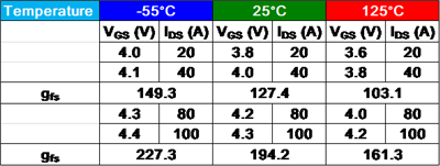
Picking data points from the data-sheet curves, Table 1 lists the estimated values for gfs. You can see that transconductance has a negative temperature coefficient.


Table 1: Estimated gfs values for the CSD17576Q5B

You can make the same gfs estimates using the transfer characteristics for the CSD19532Q5B, as listed in Table 2.


Table 2: Estimated gfs values for the CSD19532Q5B

Dynamic characteristics

Parameters in the dynamic characteristics section are an indication of the MOSFET’s switching speed. These include the parasitic capacitances (CISS, COSS and CRSS), the internal series gate resistance (RG) and the charge parameters (QG, QGD, QGS and QOSS). These parameters, along with the external gate-drive circuit, determine the typical switching times (td(on), tr, td(off) and tf). There is minimal temperature variation of the parasitic capacitances and charge parameters. RG varies with temperature but is typically swamped out by an external gate resistor and the output impedance of the gate driver, resulting in some minor deviation of the switching times specified in the data sheet. Figure 7 shows a MOSFET with the parasitic capacitances and internal series gate resistance.


Figure 7: MOSFET model with parasitic elements

Diode characteristics

The last section of the electrical characteristics table is the drain-to-source body-diode specifications. The diode forward voltage (VSD) has a negative temperature characteristic, as shown in typical MOSFET characteristics. Reverse-recovery charge (Qrr) and reverse-recovery time (trr) both increase at elevated temperatures. Because of this, reverse-recovery losses also increase at elevated temperatures.

Figure 8 shows the reverse-recovery behavior with temperature for two non-TI FETs. Qrr is the area enclosed by the drain current and trr is the time it takes for the current to return to zero. You can expect similar behavior from TI NexFET devices over temperature.

Figure 8: Reverse-recovery current vs. temperature for two FETs

Safe operating area

Engineers often ask me how to derate for temperature from the safe operating area (SOA) curves in a MOSFET data sheet. Figure 9 shows the SOA curves at TA = 25°C for the CSD17576Q5B and CSD19532Q5B.


Figure 9: Maximum safe operating area at TA = 25°C: CSD17576Q5B (a); and CSD19532Q5B (b)

The easiest approach is to use a linear derating factor. From the graph, determine the SOA current, IDS(SOA), at the voltage, VDS(SOA) and the pulse width of interest. Equation 2 calculates the SOA current at temperature T (°C) as:

IDS(SOA@T) = IDS(SOA)× (TJmax - T)/(TJmax - 25°C)                             (2)

Equation 2 yields 0 current when T = TJmax, specified in the data sheet.

Conclusion

In this technical article, I reviewed a TI NexFET data sheet, what’s in it and what’s not. I explored specifications that have a temperature dependency not included in the data sheet and provided typical curves and data showing how these specifications may vary with temperature. The examples used in this article were for two specific TI NexFET devices and showed the general trends versus temperature.

The typical curves presented in this article are to help you understand how these parameters vary with temperature, but they are no guarantee of actual performance. Always use the data-sheet limits when designing with TI FETs. If you don’t see certain specifications in the data sheet, please request them from TI in the E2E forum.

Additional resources

Reference

  1. Jahdi, Saeed, Olayiwola Alatise, Roozbeh Bonyadi, Petros Alexakis, Craig Fisher, Jose A. Ortiz Gonzalez, Li Ran, and Philip Mawby “An Analysis of the Switching Performance and Robustness of Power MOSFETs Body Diodes: A Technology Evaluation.” IEEE Transactions on Power Electronics 30, no. 5 (May 2015): pp. 2383-2394.

Improve wireless battery management with the industry’s best network availability

3 common design pitfalls when designing with Hall-effect sensors – and how to avoid them

$
0
0

Have you ever designed a circuit that didn’t quite turn out the way you expected? I know I have! In this article I’ll help you resolve three common challenges associated with Hall-effect sensors in industrial and automotive applications – rotary encoding, robust signaling and in-plane magnetic sensing.

Challenge No. 1 – you can’t get a good quadrature signature for your rotary encoding application

When trying to monitor speed and direction (clockwise or counterclockwise) in a rotary encoding application, it’s common to use two Hall-effect latches, or a dual latch. Although there could be several reasons for a poor quadrature signature, one of the most common is the placement (and misalignment) between the device and the ring magnet poles.

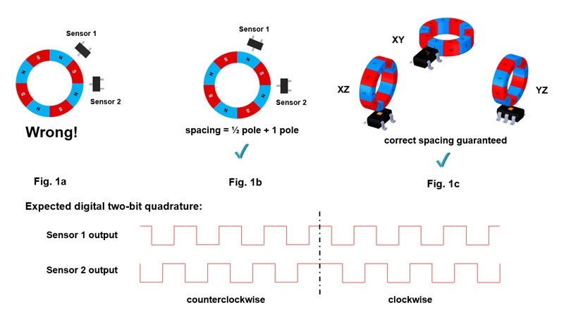
When using two Hall-effect latches, it is possible to mechanically achieve a decent two-bit quadrature output by spacing the Hall-effect sensors a half width apart from each magnet pole plus any integer number of widths. This is correctly shown in Figure 1b, where sensor 2 is located at the North/South interface, while sensor 1 is placed the width of one full pole plus a half width of the North pole away from sensor 2. For a dual Hall-effect latch, you could use a device that spaces its sensors exactly one-half the width of the magnet pole. Of course, this is very limiting because you have to match the spacing to the ring magnet poles.

Figure 1a illustrates the potential placement issues with using the two-sensor solution, while Figures 1b and 1c show how to fix it using two separate sensors or a single-chip solution, respectively. Hall-effect current sensors such as the TMAG5110 or TMAG5111 inherently help ensure a good signature for many ring magnet sizes and pole counts. Additionally, their simplicity in implementation eliminates any errors that could be introduced during mechanical placement. The precision also provides consistently accurate readings for a good quadrature signature.

Figure 1: Two-sensor rotary encoding: Fig. 1a incorrect sensor placement using two latches; Fig. 1b correct sensor placement using two latches; Fig. 1c multi-position sensor placement using a 2D sensor

Rotary encoding applications are prevalent in many automotive and industrial applications. Here are some examples:

  • Automotive – power windows, sunroofs, lift gates, sliding doors and power seats.
  • Industrial – garage door and gate openers, thermostat dials, home appliance knobs, wheel rotational sensing, and motorized window or door blinds.

Challenge No. 2 – your off-board sensor communication is not as robust as you’d like

If you’ve encountered this problem with your design, there’s a good chance you’ve used a sensor with a voltage output that has interference magnetically coupled into it. Although your trace may have been short, if there is a lot of electromagnetic interference (EMI) that you can’t account for, then your analog signaling may be coupling this interference directly into your measurement. Having a reliable link between the sensor and the microcontroller (MCU) enables the MCU to know whether the sensor is connected or disconnected. With a voltage output device, the output may be pulled to a low voltage or disconnected altogether – and the MCU will not be able to detect the difference.

EMI is extremely difficult to eliminate. Shielding, careful wire rerouting and other mitigation methods can add cost to your design. My suggested solution focuses on the sensor itself. Two-wire current-output devices are inherently less sensitive to electrical noise, making them a great option for remote sensing applications with medium-length cabling. Although sending the signal over a really long wire causes voltage losses, for most industrial and automotive applications, implementing a two-wire current-output sensor will work just fine.

Figure 2 shows how a Hall-effect switch with a two-wire current output such as the TMAG5124 can transmit a signal over a longer distance using the ground connection. “Two-wire” in this case denotes having to connect the VCC and GND from the sensor to the general-purpose input/output of the MCU. Couple the current output feature with higher precision (2mT variation in magnetic field operating and release points), and you should have a solid design.

Figure 2: Implementation of a two-wire current output sensor

Automotive applications that use a current-output sensor include:

  • Seat-belt buckles.
  • Seat position/occupancy detection.
  • Door latches.
  • Parking brakes.
  • Sunroof/trunk closures.
  • Brake pedals.

Challenge No. 3 – your Hall-effect sensor is sensitive only to orthogonal magnetic fields

Most single-axis Hall-effect sensors available today detect magnetic fields that are perpendicular to the face of the package. Your choices are limited if you need a sensor that can monitor magnetic fields parallel to the side of the package.

Figure 3 illustrates various ways to ensure horizontal magnetic field sensing. While it is possible to achieve horizontal magnetic field sensing with traditional Hall-effect sensors, there are some significant drawbacks. Mounting a standard 3-pin small outline transistor (SOT-23) package onto another smaller printed circuit board adds cost and complexity to the assembly process (Figure 3a). The transistor outlines (TO-92) package does not follow the same assembly mounting process as standard surface-mount packages, and will also add cost to the total design (Figure 3b).

If you encounter a similar situation, an in-plane Hall-effect switch like the TMAG5123-Q1 that can detect magnetic fields from the side of the surface-mount package is a good choice. It allows more freedom and flexibility in the mechanical design, because it leverages SOT-23 package and can potentially occupy a smaller space (Figure 3c).

Figure 3: Horizontal magnetic field sensing: Fig. 3a traditional sensor in SOT-23 package; Fig. 3b traditional sensor in TO-92 package; Fig. 3c in-plane sensor in SOT-23 package

Design challenges arise almost constantly, but there are usually methods or devices that can help you get around them. I hope that I’ve provided a few ways to fix some of the most common application challenges when designing with Hall-effect sensors. Comment below if you’d like to share some of your problems, and how you’ve fixed them!

Functional safety-relevant wireless communication in automotive battery management systems

$
0
0

A wireless BMS allows vehicle designers can remove heavy, expensive, maintenance-prone cabling and improve the reliability and efficiency of hybrid and electric or hybrid vehicles (HEV/EV). TI’s solution for wireless BMS empowers you to reduce the complexity of your designs, improve reliability and reduce vehicle weight to extend driving range.

To speed automakers’ development time for wireless BMS, we requested that TÜV SÜD, the industry’s leading functional safety authority, independently evaluate the quantitative and qualitative error-detection performance as well as the feasibility for automakers to achieve Automotive Safety Integrity Level (ASIL) D, the highest level of International Organization for Standardization (ISO) 26262 certification, using TI’s wireless BMS functional safety concept.

How can you transfer data in a wireless BMS while meeting functional safety requirements?

In the technical white paper, "Functional safety-relevant wireless communication in automotive battery management systems," I outline four topics to help streamline your design: 

Communications architectures for safety-relevant data transmission
Generally, there are two possible architectures for safety-relevant data transmission:

  • White channel is where complete hardware and software (including transmission protocols) are developed and validated according to functional safety standards.
  • Black channel is where end elements including HW, SW (including transmission protocol) comply with functional safety standard and part or parts of the communication channel between compliant end interfaces do not comply with any specific functional safety standard.

As described later in the white paper, TI's wireless BMS solution implements the black-channel approach by using non-compliant wireless controller chips, which also helps reduce the overall system cost.

Communication errors in wired versus wireless data transmission
One of the most important disciplines in safety-relevant data transmission is the ability of the hardware and the software to detect potential errors. Fortunately, the types of the errors and recommended approaches for detecting them have been standardized. The white paper provides a chart to make it simple to review the types of communications errors for both wired and wireless BMS.

Evaluation of detection performance for ISO 26262
Since the wireless BMS targets HEV/EV, the ISO 26262 compliance is demonstrated on the system level. The white paper outlines error detection mechanisms such as information redundancy, frame counter and timeout monitoring and points to their qualitative and quantitative evaluation.

The WP actually does not evaluate this – the full concept document does.

Implementation of communication protocols
In this section, I explain how TI's wireless BMS implements the black-channel model in compliance with IEC 62280. 


Read the white paper
to learn more about implementing functional safety in your wireless BMS design.

Three considerations for automotive powertrain safety and security

$
0
0

Jürgen Belz, senior consultant, functional safety and cybersecurity at PROMETO co-authored this technical article.

With functional safety and security concerns in automotive electronics gaining attention, including in standards bodies, it’s important for automotive designers to enable functionally safe and secure automotive electric powertrains. Functional safety, cybersecurity and high-voltage safety play an important role in the design, development and mass production of modern electric vehicles.

Functional safety

A prevalent estimate for the amount of software in a modern vehicle is between 100 and 200 million lines of code. This software runs on a large variety of programmable electronic control units and provides functions for advanced driver assistance systems and safety features in the vehicle. Examples of such systems include blind-spot monitoring, automatic emergency brakes and adaptive cruise control. Vehicles with autonomous and electric features require functional safety for safe operation.

Cybersecurity

The increasing sophistication in the type and amount of connectivity available makes vehicles more vulnerable to digital attacks. What was once considered the gold standard in the prevention of cyberattacks is no longer valid. Given the implementation of communications protocols like Controller Area Network and Bluetooth®, and now Global System for Mobile Communications and Wi-Fi® networks for vehicle-to-vehicle communication, automobiles are no longer protected by the “air gap” between them and networks that hackers may employ. Imagine a scenario where a hacker immobilizes a vehicle and only unlocks it after being paid a ransom in bitcoin.

High voltage

Additionally, all aspects of the electric drivetrain – such as the onboard charger, high-voltage to high-voltage or high-voltage to low-voltage DC/DC converter, and electric vehicle traction inverter – all use programmable microcontrollers (MCUs) such as C2000™ real-time MCUs. And with electric vehicle battery voltages approaching 600 to 800 V, it is equally important to understand and apply the requirements for high-voltage safety systems.

Automotive safety and security standards

These international standards address safety and security aspects:

  • International Organization for Standardization (ISO) 26262:2018 outlines the functional safety requirements of road vehicles.
  • ISO 6469:2018 specifies high-voltage electrical safety requirements for electrically propelled road vehicles.
  • United Nations Economic Commission for Europe WP29:2020 details automotive cybersecurity requirements for automakers worldwide.

Additionally, automotive Tier 1s (subsystem manufacturers) follow:

  • ISO DIS 21434:2020, which is still a draft international standard and a superset of Society of Automotive Engineers (SAE) J3061. ISO DIS 21434:2020 outlines a cybersecurity management framework and activities in deference to the ISO 26262 functional safety-compliant V-model-based product development life cycle.
  • SAE J3061:2016, the original “Cybersecurity Guidebook for Cyber-Physical Vehicle Systems” on which ISO/SAE DIS 21434 is based.

Electric vehicle system designers must consider aspects of all three safety and security measures.

ISO 26262 defines four automotive safety integrity levels (ASILs), as listed in Table 1.

ASIL class

Single-point fault metric

Latent fault metric

Probabilistic metric for hardware random fails

ASIL A

n/a

n/a

n/a

ASIL B

≥90%

≥60%

≤100 failure in time (FIT)

ASIL C

≥97%

≥80%

≤100 FIT

ASIL D

≥99%

≥90%

≤10 FIT

Table 1: ISO 26262 quantitative random hardware diagnostic coverage metrics per each ASIL class

ISO/SAE 21434 defines four cybersecurity assurance levels (CALs) based on attack vector and impact, as listed in Table 2.


Attack vector


Physical

Local

Adjacent

Network

Impact

Negligible

n/a

n/a

n/a

n/a

Moderate

CAL 1

CAL 1

CAL 2

CAL 3

Major

CAL 1

CAL 2

CAL 3

CAL 4

Severe

CAL2

CAL 3

CAL 4

CAL 4

Table 2: ISO/SAE 21434 cybersecurity assurance levels


SAE J3061 defines four cybersecurity integrity levels (CSILs) and recommends the application of a cybersecurity process for all automotive systems responsible for functions that are ASIL rated per ISO 26262, or for functions associated with subsystems such as propulsion, braking and steering. These are CSIL A, CSIL B, CSIL C and CSIL D.

ISO 6469 describes four classes that depend on the maximum working voltage range “U” of an electric circuit, as listed in Table 3.

Voltage class

Highest (maximum) working voltage

DC voltage (in V)

AC voltage (in root-mean-square value)

A

0 < U ≤ 60

0 < U ≤ 30

B

60 < U ≤ 1,500

30 < U ≤ 1,000

B1

60 < U ≤ 75

30 < U ≤ 50

B2

75 < U ≤ 1,500

50 < U ≤ 1,000

Table 3: ISO 6469 permissible maximum voltage levels per each voltage class


There is significant synergy between ISO 21434 and ISO 26262 in terms of how to implement their recommendations during the design, development and mass production of an electrical/electronic/programmable electronic system. 

Conclusion

With the increasing complexity of automotive subsystems in hybrid electric vehicles and electric vehicles and the electrification of the powertrain, safety and security are becoming higher priorities. Fortunately, commonly accepted normative international standards address these safety and security aspects.

 TI can help you make security and safety assessments and achieve security and safety goals in your automotive designs. For example, while developing a powertrain solution with a C2000™ real-time MCU, the online safety material is a great starting point.

Additional resources

Viewing all 4543 articles
Browse latest View live


<script src="https://jsc.adskeeper.com/r/s/rssing.com.1596347.js" async> </script>